
Introduction
This is the chapter web page to support the content in Chapter 15 of the book: Exploring BeagleBone – Tools and Techniques for Building with Embedded Linux. The summary introduction to the chapter is as follows:
The Beagle board AM335x SoC contains two programmable real-time units (PRUs) that can be used for certain real-time operations, and these are the focus of this chapter. The chapter begins with input and output examples that help explain the operation of the PRUs and their encompassing industrial communication subsystem (PRU-ICSS). The real-time capabilities of the AM335x are demonstrated using two applications—the first generates custom waveforms on a GPIO, and the second uses a low-cost ultrasonic distance sensor that requires precise timing in order to communicate the distance to an obstacle.
Learning Outcomes
After completing this chapter, you should be able to do the following:
- Describe real-time kernel and hardware solutions that can be used on the Beagle boards.
- Use tools such as the PRU Debugger and Texas Instruments’ PRU Code Generation Tools (CGT) for PRU-ICSS application development.
- Write a PRU program that can flash an LED and transfer it to the PRU-ICSS using remoteproc.
- Describe the important features of the PRU-ICSS, such as its structure, registers, memory addressing, and assembly language instructions.
- Write a PRU program that shares memory with a Linux host application.
- Write a PRU program that interfaces to regular GPIOs that are in Linux host space.
- Write a PRU program that generates PWM signals, and adapt it to output user-defined analog waveforms on a GPIO pin.
- Apply the PRU to sensor interfacing applications for which time measurement is important, such as interfacing to ultrasonic distance sensors.
Digital Media Resources
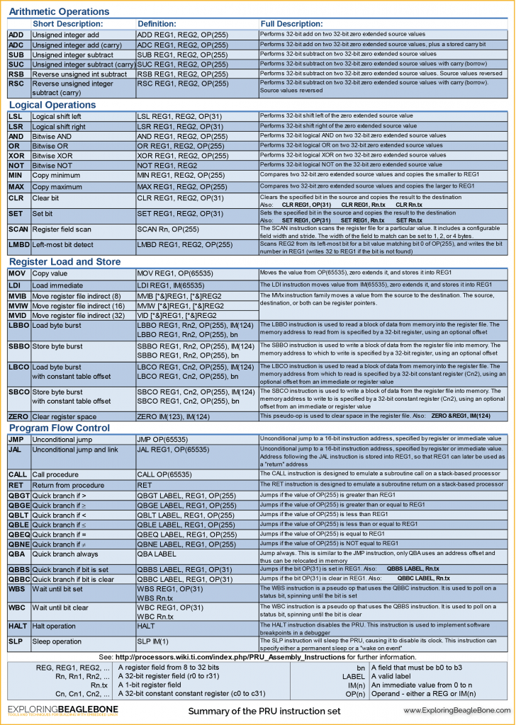
The PRU Instruction Set Summary
This summary sheet was created with permission from information that is courtesy of Texas Instruments. It is a version of Figure 13-7 of the book:
- The PRU Instruction Summary Sheet [PDF Format (0.1MB)] [PNG Format (0.8MB)]
Additional Content for First Edition
When possible I am adding additional content to this website to support the book by tackling different topics, in particular those topics:
- that could not be covered within the time frame of the development of the book due to their complexity or specificity,
- that are subject to so much change that a book could not reasonably capture those changes and remain up to date,
- that could not be covered within the page numbers available in order to keep the price of the book reasonable.
In this section two main topics are covered in detail: High-speed Analog-to-Digital Conversion using the PRU-ICSS (an advanced topic) and Clock-Signal Generator Circuits using the PRU-ICSS.
High-Speed Analog to Digital Conversion (ADC) using the PRU-ICSS
The MCP3008 8-Channel 10-bit ADC (100kSps max)
[Added February 2015] Chapter 13 in the book describes the operation of the PRU-ICSS and provides several different examples for reading and writing from/to GPIOs, including high-speed digital interfacing examples. However, one topic that is not covered is high-speed analog sampling. As described in the chapter, the PRU-ICSS is a very powerful device but it does not have straightforward access to the AM335x’s on-board ADC.
This is a complex topic and it should not be your first interaction with the PRU-ICSS. Please review the earlier examples in Chapter 13 before tackling this topic. It is the most challenging PRU-ICSS code that I have written to date – the final outcome may seem reasonably straightforward, but there were several incorrect intermediate versions (several!).
This example utilizes the work that is described in Chapter 8 – in particular, the additional content that was added in January 2015 on an “SPI Analog to Digital Converter (ADC) Example”. I have purposefully structured it this way, so that you can build, test and become familiar with the limitations of the circuit in Chapter 8 before progressing to this, the high-speed version.
The MCP3008 is used again for the first version of this circuit. It is a low-cost PDIP chip that has eight selectable channels. This fact allows for a breadboard implementation, but there are more advanced ICs available (generally surface mounted), such as the ADS7883.
Here are the features of the solution that is presented in this discussion:
-
- It has a configurable sampling rate – up to 100KSps with this IC. The sampling rate can be configured from within Linux userspace. Higher sample rates are possible with alternative ADCs (to follow soon).
-
- The samples can be captured free from jitter. Both PRUs are employed in order to achieve this.
-
- The input channel on the MCP3008 and the single-ended/differential inputs can be chosen and configured from Linux userspace.
-
- The quantity of data to be captured can be configured from Linux userspace and it is not limited by the relatively low PRU memory space size. The current solution is limited by the amount of unused DDR memory.
-
- The PRU programs automatically determine Linux memory addresses and size limitations.
-
- The program supports 10-bit, 12-bit and 16-bit ADCs (The MCP3008 is a 10-bit ADC).
- A custom device tree overlay (DTO) is made available for this example.
Here are the current downsides of the code example that is presented in this solution:
-
- The sample duration is currently limited by the amount of DDR memory made available to the PRU-ICSS (this can be many megabytes). I have not written the userspace code to “consume” the samples as they arrive in Linux userspace (I don’t think it is overly problematic – that task is marked TODO).
-
- The code has not been overly optimized (for pedagogical reasons) – it’s still fast enough!
- The sampling rate is regular (jitter free), but the rate isn’t necessarily precise (e.g., 100kHz might be 100.01kHz and will always be 100.01kHz) – if you have a very specific rate in mind for your application then you can tweak the code to achieve a very precise rate (with 5ns period increments).
The Circuit
-
- P9_27 pr1_pru0_pru_r30_5 SPI_CS0 (Chip Select) – The chip select is used to initiate communication with the MCP3008. This is an active-low line that must be brought low in order to capture a sample. This line must be set high in between each sample.
-
- P9_30 pr1_pru0_pru_r30_2 SPI_SCLK (CLK) – This is the data transfer clock (This is NOT the ADC sample clock). The BeagleBone PRU code generates this data transfer clock, which synchronizes communication between the BBB and the MCP3008.
-
- P9_29 pr1_pru0_pru_r30_1 SPI_D1 (MOSI) – Master out, Slave in. This line is used by the BBB PRU code to configure the MCP3008 (i.e., select which input and the ADC type – for example, to select single-ended mode on Channel 0, we can send 0x01 0x80 0x00)
- P9_28 pr1_pru0_pru_r31_3 SPI_D0 (MISO) – Master in, Slave out. This line is used by the MCP3008 to transfer a 10-bit sample back to the BBB. The MOSI and MISO lines communicate data simultaneously.
Any PRU input/output pins can be used for this task – there is nothing unique about the particular PRU pins that are chosen in this example (i.e., there is no special SPI communication functionality on these pins). The colors of the lines are kept consistent throughout this example.
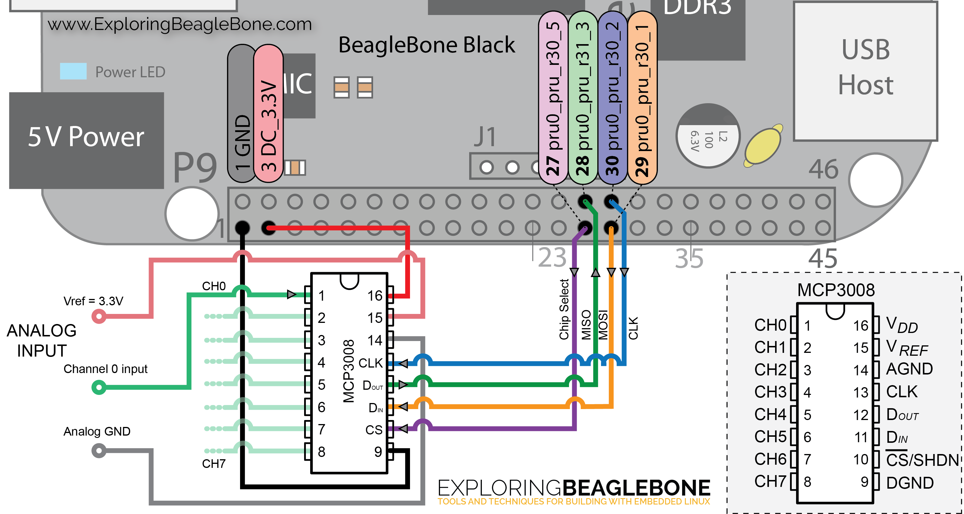
Figure 13.A1: The PRU-ICSS ADC circuit (click any figure in this section for a high-resolution version)
A device tree overlay (DTO) is available to configure the pins correctly (see Listing 13.A1). The pins are configured by using the tables in Chapter 6. There is no requirement for pull-up/down resistors in this case, so they have not been enabled. Remember from the discussion in Chapter 13 that pru0 designated pins are accessible from PRU0, and pru1 designated pins are accessible from PRU1. In this solution the SPI code is executed on PRU0 and the timer code is executed on PRU1. Also, remember that r30 refers to an output, and r31 refers to an input; hence, pin Mode 5 and Mode 6 are chosen as follows:
- 0x1a4 0x0d // CS P9_27 pr1_pru0_pru_r30_5, MODE5 | OUTPUT | DIS 00001101=0x0d
- 0x19c 0x2e // MISO P9_28 pr1_pru0_pru_r31_3, MODE6 | INPUT | DIS 00101110=0x2e
- 0x194 0x0d // MOSI P9_29 pr1_pru0_pru_r30_1, MODE5 | OUTPUT | DIS 00001101=0x0d
- 0x198 0x0d // CLK P9_30 pr1_pru0_pru_r30_2, MODE5 | OUTPUT | DIS 00001101=0x0d
- 0x0a4 0x0d // SAMP P8_46 pr1_pru1_pru_r30_1, MODE5 | OUTPUT | DIS 00001101=0x0d
The last entry in the device tree overlay is purely for testing and can be removed. This test output can be used to test that the code on PRU1 is working correctly by connecting P8_46 to an oscilloscope or logic analyzer in order to validate the clock pulse signal.
Listing 13.A1: The Device Tree Overlay for this Example
/* Device Tree Overlay for enabling the pins that are used in the Chapter 13
* additional material example on High-Speed Analog to Digital Conversion (ADC)
* using the PRU-ICSS. This overlay is based on the BB-PRU-01 overlay
* Written by Derek Molloy for the book "Exploring BeagleBone: Tools and
* Techniques for Building with Embedded Linux" by John Wiley & Sons, 2014
* ISBN 9781118935125. Please see the file README.md in the repository root
* directory for copyright and GNU GPLv3 license information.
*/
/dts-v1/;
/plugin/;

/ {
   compatible = "ti,beaglebone", "ti,beaglebone-black";

   part-number = "EBB-PRU-ADC";
   version = "00A0";

   /* This overlay uses the following resources */
   exclusive-use =
          "P9.27", "P9.28", "P9.29", "P9.30", "P8.46", "pru0", "pru1";

   fragment@0 {
      target = <&am33xx_pinmux>;
      __overlay__ {

         pru_pru_pins: pinmux_pru_pru_pins {   // The PRU pin modes
            pinctrl-single,pins = <
	       // See Table 6-7, no pull up/down resistors enabled
               0x1a4 0x0d  // CS   P9_27 pr1_pru0_pru_r30_5, MODE5 | OUTPUT | DIS  00001101=0x0d
               0x19c 0x2e  // MISO P9_28 pr1_pru0_pru_r31_3, MODE6 | INPUT  | DIS  00101110=0x2e
               0x194 0x0d  // MOSI P9_29 pr1_pru0_pru_r30_1, MODE5 | OUTPUT | DIS  00001101=0x0d
               0x198 0x0d  // CLK  P9_30 pr1_pru0_pru_r30_2, MODE5 | OUTPUT | DIS  00001101=0x0d
	       // This is for PRU1, the sample clock -- debug only
               0x0a4 0x0d  // SAMP P8_46 pr1_pru1_pru_r30_1, MODE5 | OUTPUT | DIS  00001101=0x0d
            >;
         };
      };
   };

   fragment@1 {         // Enable the PRUSS
      target = <&pruss>;
      __overlay__ {
         status = "okay";
         pinctrl-names = "default";
         pinctrl-0 = <&pru_pru_pins>;
      };
   };

};
The Programs
| 1 | Load the Device Tree Overlay (virtual cape) as above. |
| 2 | Allocate DDR external RAM for the sample data using Linux userspace kernel module tools. |
| 3 | The main Linux executable (pruadc). This program loads the two PRU programs into the PRU-ICSS transfers the configuration to the PRU memory spaces and starts the execution of both PRU programs. The source code is in PRUADC.c |
| 4 | The PRU ADC code (bin). This program is placed in PRU0 and it performs the sampling role by communicating via SPI to the MCP3008. It also transfers the sample data back to Linux userspace DDR external RAM. The source code is in PRUADC.p |
| 5 | The PRU sample clock (bin). This program acts as an internal sample clock. Its frequency can be configured from Linux userspace. If you wish to preserve this PRU you could replace this functionality with the use of an external crystal oscillator. The source code is in PRUClock.p |
| 6 | The Memory -> File program (mem2file). This Linux userspace program takes the samples from DDR external RAM and outputs them to the standard output which can be re-directed to a file. The source code is in mem2file.c (this program is based on the devmem2 program that is discussed throughout the book). |
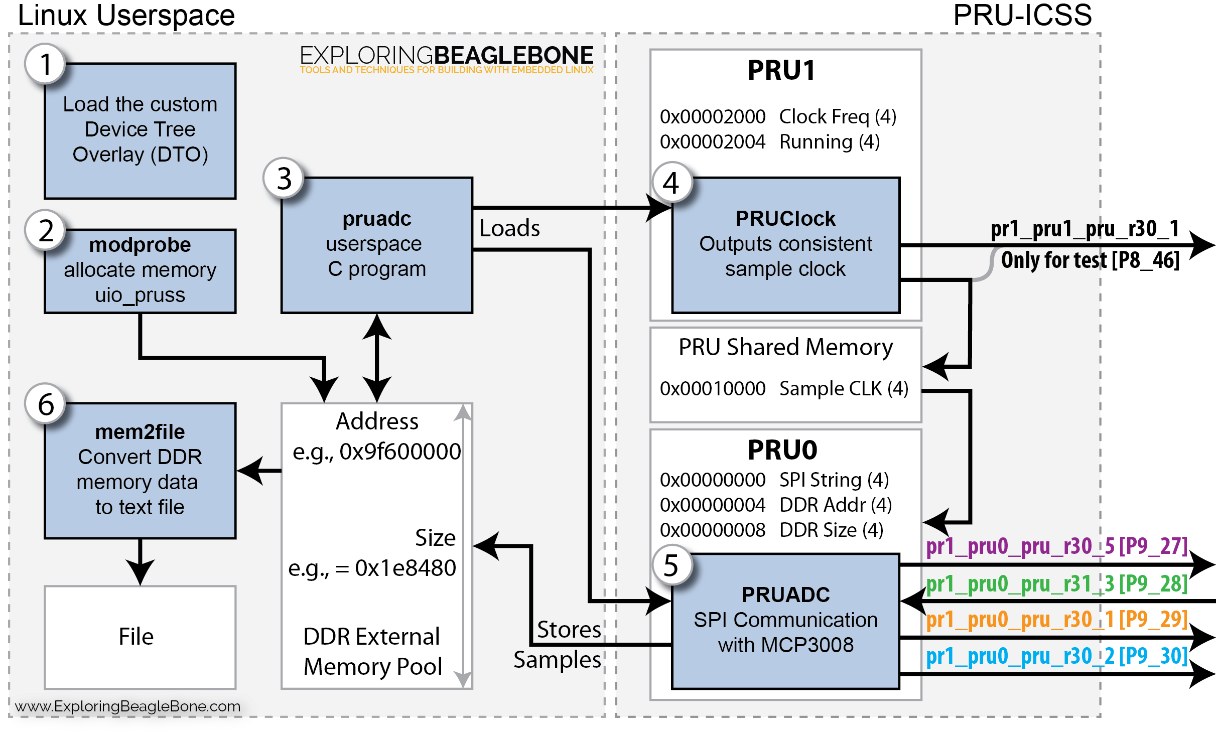 Figure 13.A2: The structure and interaction between the various programs (click any figure in this section for a high-resolution version)The steps/programs are identified in Figure 13.A2 above and are now described below: Step 1. The DTO must be loaded for this code to be executed. As before, please disable the HDMI overlay, using the steps in the chapter, and use the following steps and check that the overlay has loaded correctly:
root@beaglebone:~/exploringBB/chp13/adc# cp EBB-PRU-ADC-00A0.dtbo /lib/firmware/
root@beaglebone:~/exploringBB/chp13/adc# cd /lib/firmware/
root@beaglebone:/lib/firmware# echo EBB-PRU-ADC > $SLOTS
root@beaglebone:/lib/firmware# cat $SLOTS
 0: 54:PF---
 1: 55:PF---
 2: 56:PF---
 3: 57:PF---
 4: ff:P-O-L Bone-LT-eMMC-2G,00A0,Texas Instrument,BB-BONE-EMMC-2G
 5: ff:P-O-- Bone-Black-HDMI,00A0,Texas Instrument,BB-BONELT-HDMI
 6: ff:P-O-- Bone-Black-HDMIN,00A0,Texas Instrument,BB-BONELT-HDMIN
 7: ff:P-O-L Override Board Name,00A0,Override Manuf,EBB-PRU-ADC
Step 2. The PRU-ICSS has a UIO driver that exports host event out interrupts, L3 RAM and DDR RAM to Linux userspace so that applications can interact with the PRU-ICSS. This driver is automatically loaded when the device tree overlay is loaded in Step 1. You can see this by using the lsmod command:
root@beaglebone:~/exploringBB/chp13/adc# lsmod
Module                  Size  Used by
uio_pruss               4066  0
g_multi                50407  2
libcomposite           15028  1 g_multi
mt7601Usta            641118  0
The module can be unloaded from the Linux kernel using the rmmod application so that we can reload it and alter its behavior:
root@beaglebone:~/exploringBB/chp13/adc# rmmod uio_pruss
root@beaglebone:~/exploringBB/chp13/adc# lsmod
Module                  Size  Used by
g_multi                50407  2
libcomposite           15028  1 g_multi
mt7601Usta            641118  0
The modprobe application can then be used to add the module back to the Linux kernel, however with the DDR external RAM size updated to a larger value. In this example a pool of 2,000,000 bytes is allocated for the sample data (i.e., 1 million 16-bit samples). 2,000,000 is 0x1E8480 in hexadecimal. The source code of uio_pruss.c can be used to identify module parameters, where you can see two parameters:
-
- sram_pool_sz – SRAM pool size to allocate (default 16K).
- extram_pool_sz – The external RAM pool size to allocate (default 256K).
The external RAM pool size can be modified as follows:
root@beaglebone:~/exploringBB/chp13/adc# modprobe uio_pruss extram_pool_sz=0x1E8480
root@beaglebone:~/exploringBB/chp13/adc# lsmod
Module                  Size  Used by
uio_pruss               4066  0
g_multi                50407  2
libcomposite           15028  1 g_multi
mt7601Usta            641118  0
This modification can be tested using sysfs, as follows:
root@beaglebone:~/exploringBB/chp13/adc# cd /sys/class/uio/uio0/maps/map1
root@beaglebone:/sys/class/uio/uio0/maps/map1# ls
addr  name  offset  size
root@beaglebone:/sys/class/uio/uio0/maps/map1# cat addr
0x9f600000
root@beaglebone:/sys/class/uio/uio0/maps/map1# cat size
0x1e8480
You can see that the size is set correctly and the base address is 0x9f600000 (this will vary). The pruadc.c program loads these values automatically using sysfs and transfers them to PRU0 memory (0x00000004 and 0x00000008) so that the PRUADC program can write directly to this external RAM pool in Linux userspace, directly from PRU0.
Please note that Step 2 was motivated and informed by the excellent work by Elias Bakken at Hipstercircuits.
Step 3. The pruadc program can be executed. This program loads the two PRU binaries (PRUClock.bin and PRUADC.bin) and loads them into PRU1 and PRU0 respectively. The source code for pruadc.c is provided in Listing 13.A2 below. You can see that the program also loads configuration values into PRU memory as follows:
- The SPI Command String (4 bytes in PRU0 memory 0x00000000) – this value is the command that is sent from the BBB to the MCP3008. In the example, this is 0x01800000, where the six first most significant bytes are used. Note, you will see this exact same string of data used in the example in the additional materials in Chapter 8.
- The DDR Address (4 bytes in PRU0 memory 0x00000004) – this value is the base address of the DDR external RAM pool so that the PRU0 can write directly to this memory space in order to store sample data. This avoids the tight limits in PRU memory space. In this example case the address is 0x9f600000 and this is determined automatically using sysfs (as above).
- The DDR Size (4 bytes in PRU0 memory 0x00000008) – this value is the size of the DDR external RAM pool. This is determined automatically using sysfs (as above) and has the size 0x1E8480 in this example (i.e., 2,000,000 bytes).
- The Clock Frequency (4 bytes in PRU1 memory 0x00002000) – this value is a period that is proportional to the sample clock frequency. There is a struct in pruadc.c that provides some sample periods (e.g., FREQ_100kHz).
- The Clock Running flag (4 bytes in PRU1 memory 0x00002004) – the two LSBs of this value allow for the clock to be turned on/off or updated from Linux userspace, as described in the PRU Clock Example above.
- The Sample Clock value (4 bytes in PRU shared memory 0x00010000) – this value is shared between PRU0 and PRU1 and allows the PRU0 to capture a sample whenever the clock that is driven by PRU1 generates a rising edge.
When this program is executed the PRUADC program captures 1 million 16-bit samples at a sample rate of 100KSps. Therefore, it takes about 10 seconds to execute. The program can be executed as follows:
root@beaglebone:~/exploringBB/chp13/adc# ./pruadc
The PRU clock state is set as period: 495 (0x1ef) and state: 1
-> the PRUClock memory is mapped at the base address: 4a302000
-> the PRUClock on/off state is mapped at address: 4a310000
Sending the SPI Control Data: 0x1800000
The DDR External Memory pool has location: 0x9f600000 and size: 0x1e8480 bytes
-> this space has capacity to store 1000000 16-bit samples (max)
EBBClock PRU1 program now running (495)
EBBADC PRU0 program completed, event number 12.
Listing 13.A2: The PRUADC.c Program Listing (please note that you can expand or open the code in a new window using the controls in the top-right of the display box)
/*  This program loads the two PRU programs into the PRU-ICSS transfers the configuration
*   to the PRU memory spaces and starts the execution of both PRU programs.
*   pressed. By Derek Molloy, for the book Exploring BeagleBone. Please see:
*        www.exploringbeaglebone.com/chapter13
*   for a full description of this code example and the associated programs.
*/

#include <stdio.h>
#include <stdlib.h>
#include <prussdrv.h>
#include <pruss_intc_mapping.h>

#define ADC_PRU_NUM	   0   // using PRU0 for the ADC capture
#define CLK_PRU_NUM	   1   // using PRU1 for the sample clock
#define MMAP0_LOC   "/sys/class/uio/uio0/maps/map0/"
#define MMAP1_LOC   "/sys/class/uio/uio0/maps/map1/"

enum FREQUENCY {    // measured and calibrated, but can be calculated
	FREQ_12_5MHz =  1,
	FREQ_6_25MHz =  5,
	FREQ_5MHz    =  7,
	FREQ_3_85MHz = 10,
	FREQ_1MHz   =  45,
	FREQ_500kHz =  95,
	FREQ_250kHz = 245,
	FREQ_100kHz = 495,
	FREQ_25kHz = 1995,
	FREQ_10kHz = 4995,
	FREQ_5kHz =  9995,
	FREQ_2kHz = 24995,
	FREQ_1kHz = 49995
};

enum CONTROL {
	PAUSED = 0,
	RUNNING = 1,
	UPDATE = 3
};

// Short function to load a single unsigned int from a sysfs entry
unsigned int readFileValue(char filename[]){
   FILE* fp;
   unsigned int value = 0;
   fp = fopen(filename, "rt");
   fscanf(fp, "%x", &value);
   fclose(fp);
   return value;
}

int main (void)
{
   if(getuid()!=0){
      printf("You must run this program as root. Exiting.\n");
      exit(EXIT_FAILURE);
   }
   // Initialize structure used by prussdrv_pruintc_intc
   // PRUSS_INTC_INITDATA is found in pruss_intc_mapping.h
   tpruss_intc_initdata pruss_intc_initdata = PRUSS_INTC_INITDATA;

   // Read in the location and address of the shared memory. This value changes
   // each time a new block of memory is allocated.
   unsigned int timerData[2];
   timerData[0] = FREQ_100kHz;
   timerData[1] = RUNNING;
   printf("The PRU clock state is set as period: %d (0x%x) and state: %d\n", timerData[0], timerData[0], timerData[1]);
   unsigned int PRU_data_addr = readFileValue(MMAP0_LOC "addr");
   printf("-> the PRUClock memory is mapped at the base address: %x\n", (PRU_data_addr + 0x2000));
   printf("-> the PRUClock on/off state is mapped at address: %x\n", (PRU_data_addr + 0x10000));

   // data for PRU0 based on the MCPXXXX datasheet
   unsigned int spiData[3];
   spiData[0] = 0x01800000;
   spiData[1] = readFileValue(MMAP1_LOC "addr");
   spiData[2] = readFileValue(MMAP1_LOC "size");
   printf("Sending the SPI Control Data: 0x%x\n", spiData[0]);
   printf("The DDR External Memory pool has location: 0x%x and size: 0x%x bytes\n", spiData[1], spiData[2]);
   int numberSamples = spiData[2]/2;
   printf("-> this space has capacity to store %d 16-bit samples (max)\n", numberSamples);

   // Allocate and initialize memory
   prussdrv_init ();
   prussdrv_open (PRU_EVTOUT_0);

   // Write the address and size into PRU0 Data RAM0. You can edit the value to
   // PRUSS0_PRU1_DATARAM if you wish to write to PRU1
   prussdrv_pru_write_memory(PRUSS0_PRU0_DATARAM, 0, spiData, 12);  // spi code
   prussdrv_pru_write_memory(PRUSS0_PRU1_DATARAM, 0, timerData, 8); // sample clock

   // Map the PRU's interrupts
   prussdrv_pruintc_init(&pruss_intc_initdata);

   // Load and execute the PRU program on the PRU
   prussdrv_exec_program (ADC_PRU_NUM, "./PRUADC.bin");
   prussdrv_exec_program (CLK_PRU_NUM, "./PRUClock.bin");
   printf("EBBClock PRU1 program now running (%d)\n", timerData[0]);

   // Wait for event completion from PRU, returns the PRU_EVTOUT_0 number
   int n = prussdrv_pru_wait_event (PRU_EVTOUT_0);
   printf("EBBADC PRU0 program completed, event number %d.\n", n);

// Disable PRU and close memory mappings
   prussdrv_pru_disable(ADC_PRU_NUM);
   prussdrv_pru_disable(CLK_PRU_NUM);

   prussdrv_exit ();
   return EXIT_SUCCESS;
}
// PRU1 program to provide a variable frequency clock on P8_46 (pru1_pru_r30_1)
// that is controlled from Linux userspace by setting the PRU memory state. This
// program is executed on PRU1 and outputs the sample clock on P8_46. If you wish
// to change the clock to output on a different pin edit the code. The program is
// memory controlled using the first two 4-byte numbers in PRU memory space:
// - The delay is set in memory address 0x00000000 (4 bytes long)
// - The counter can be turned on and off by setting the LSB of 0x00000004 (4 bytes)
//   to 1 (on) or 0 (off)
// - The delay value can be updated by setting the second most LSB to 1 (it will
//   immediately return to 1) e.g., set 0x00000004 to be 3, which will return to 1
//   to indicate that the update has been performed.
// This program was writen by Derek Molloy to align with the content of the book
// Exploring BeagleBone, 2014. This example was written after publication.

.origin 0                        // start of program in PRU memory
.entrypoint START                // program entry point (for a debugger)

START:	                         // aims to load the clock period value into r2
	MOV	r1, 0x00000000	 // load the base address into r1
	LBBO	r2, r1, 0, 4	 // the clock delay is now loaded into r2. 4 bytes.
	MOV	r4, 0x00010000   // Going to use PRU shared memory to share the state change
	MOV	r5, r1		 // r5 going to store the state of the clock i.e. high/low
	QBA	ENDOFLOOP	 // move to comparison -- avoids duplicating code

MAINLOOP:
	CLR	r30.t1           // set the sample clock signal to be low
	CLR	r5.t00
	SBBO    r5, r4, 0, 4	 // store the clock state in PRU shared memory
	MOV	r0, r2		 // load the delay r2 into temp r0 (50% duty cycle)
	ADD	r0, r0, 1	 // balance duty cycle by looping 1 extra time on low

DELAYOFF:
	SUB	r0, r0, 1	 // decrement the counter by 1 and loop (next line)
	QBNE	DELAYOFF, r0, 0  // loop until the delay has expired (i.e., equals 0)
				 // next instruction order used to keep 50% duty cycle
	MOV	r0, r2           // re-load the delay r2 into temporary r0
	SET	r30.t1		 // set the sample clock to be high
	SET	r5.t00
	SBBO    r5, r4, 0, 4	 // store the clock state in PRU shared memory

DELAYON:
	SUB	r0, r0, 1	 // decrement the counter by 1 and loop (next line)
	QBNE	DELAYON, r0, 0   // loop until the delay has expired (equals 0)

ENDOFLOOP:                       // is the clock running?
	LBBO	r3, r1, 4, 4	 // loaded the state into r3 -- is running? 4 bytes total
	QBBS	RESETCLK, r3.t1	 // If r3 bit 1 is high then reload the clock period
	QBBS	MAINLOOP, r3.t0  // If r3 bit 0 is high then the clock is running
	QBA	ENDOFLOOP        // otherwise loop without toggling the clock -- i.e. clock off

RESETCLK:			 // clear the r3.t1 bit and write back to memory
				 // indicating that the clock frequency has been updated
	CLR	r3, r3.t1	 // i.e., clear the reload clock flag
	SBBO	r3, r1, 4, 4     // write that value back into memory
	QBA	START            // go back to the start of the program

END:				 // program will not exit due to the QBA on the line above
	HALT                     // halt the pru program -- never reached!
Please note that there is a full discussion on PRU-based clocks in the next section below (PRU-based Clock Signal Generators).
Step 5. The PRUADC PRU program (in Listing 13.A4) is executed automatically when the pruadc program executes. The source code writes 24 bits to the MOSI pin (P9_29) on the rising edge of the data clock pulse (P9_30) and simultaneously reads 24 bits from the MISO pin (P9_28) on the falling edge of the data clock pulse. The CS pin is pulled low (P9_27) to instigate a sample request. This pin must go high between each requested sample. Figure 13.A3 illustrates the data transaction that takes place between the PRUADC program and the MCP3008. Again, this is based on the code that is presented in the additional material in Chapter 8.
Listing 13.A4: The PRUADC.p Program Listing
// PRU program to communicate to the MCPXXXX family of SPI ADC ICs. The program
// generates the SPI signals that are required to receive samples. To use this
// program as is, use the following wiring configuration:
//   Chip Select (CS):   P9_27    pr1_pru0_pru_r30_5  r30.t5
//   MOSI            :   P9_29    pr1_pru0_pru_r30_1  r30.t1
//   MISO            :   P9_28    pr1_pru0_pru_r31_3  r31.t3
//   CLK             :   P9_30    pr1_pru0_pru_r30_2  r30.t2
//   Sample Clock    :   P8_46    pr1_pru1_pru_r30_1  -- for testing only
// This program was writen by Derek Molloy to align with the content of the book
// Exploring BeagleBone. See exploringbeaglebone.com/chapter13/

.setcallreg  r29.w2		 // set a non-default CALL/RET register
.origin 0                        // start of program in PRU memory
.entrypoint START                // program entry point (for a debugger)

#define PRU0_R31_VEC_VALID 32    // allows notification of program completion
#define PRU_EVTOUT_0    3        // the event number that is sent back

// Constants from the MCP3004/3008 datasheet
#define TIME_CLOCK      12       // T_hi and t_lo = 125ns = 25 instructions (min)

START:
        // Enable the OCP master port -- allows transfer of data to Linux userspace
	LBCO    r0, C4, 4, 4     // load SYSCFG reg into r0 (use c4 const addr)
	CLR     r0, r0, 4        // clear bit 4 (STANDBY_INIT)
	SBCO    r0, C4, 4, 4     // store the modified r0 back at the load addr

	MOV	r1, 0x00000000	 // load the base address into r1
				 // PRU memory 0x00 stores the SPI command - e.g., 0x01 0x80 0x00
				 // the SGL/DIFF and D2, D1, D0 are the four LSBs of byte 1 - e.g. 0x80
	MOV	r7, 0x000003FF	 // the bit mask to use on the returned data (i.e., keep 10 LSBs only)
	LBBO    r8, r1, 4, 4     // load the Linux address that is passed into r8 -- to store sample values
	LBBO	r9, r1, 8, 4	 // load the size that is passed into r9 -- the number of samples to take

	MOV	r3, 0x00000000	 // clear r3 to receive the response from the MCP3XXX
	CLR	r30.t1		 // clear the data out line - MOSI

GET_SAMPLE:			 // load the send value on each sample, allows sampling re-configuration
	LBBO	r2, r1, 0, 4	 // the MCP3XXX states are now stored in r2 -- need the 16 MSBs

	// Need to wait at this point until it is ready to take a sample - i.e., 0x00010000
	// store the address in r5
	MOV	r5, 0x00010000   // LSB of value at this address is the clock flag
SAMPLE_WAIT_HIGH:		 // wait until the PRU1 sample clock goes high
	LBBO	r6, r5, 0, 4	 // load the value at address r5 into r6
	QBNE	SAMPLE_WAIT_HIGH, r6, 1 // if the

	CLR	r30.t5		 // set the CS line low (active low)
	MOV	r4, 24		 // going to write/read 24 bits (3 bytes)
SPICLK_BIT:                      // loop for each of the 24 bits
	SUB	r4, r4, 1        // count down through the bits
	CALL	SPICLK           // repeat call the SPICLK procedure until all 24-bits written/read
	QBNE	SPICLK_BIT, r4, 0

	SET	r30.t5		 // pull the CS line high (end of sample)
	LSR	r3, r3, 1        // SPICLK shifts left too many times left, shift right once
	AND	r3, r3, r7	 // AND the data with mask to give only the 10 LSBs
	//SBBO	r3, r1, 12, 4    // store the data for debugging only -- REMOVE

STORE_DATA:                      // store the sample value in memory
	SUB	r9, r9, 2	 // reducing the number of samples - 2 bytes per sample
	SBBO	r3.w0, r8, 0, 2	 // store the value r3 in memory
	ADD	r8, r8, 2	 // shifting by 2 bytes - 2 bytes per sample
	QBEQ	END, r9, 0       // have taken the full set of samples

SAMPLE_WAIT_LOW:                 // need to wait here if the sample clock has not gone low
	LBBO	r6, r5, 0, 4	 // load the value in PRU1 sample clock address r5 into r6
	QBNE	SAMPLE_WAIT_LOW, r6, 0 // wait until the sample clock goes low (just in case)
	QBA	GET_SAMPLE
END:
	MOV	r31.b0, PRU0_R31_VEC_VALID | PRU_EVTOUT_0
	HALT                     // End of program -- below are the "procedures"


// This procedure applies an SPI clock cycle to the SPI clock and on the rising edge of the clock
// it writes the current MSB bit in r2 (i.e. r31) to the MOSI pin. On the falling edge, it reads
// the input from MISO and stores it in the LSB of r3.
// The clock cycle is determined by the datasheet of the product where TIME_CLOCK is the
// time that the clock must remain low and the time it must remain high (assuming 50% duty cycle)
// The input and output data is shifted left on each clock cycle

SPICLK:
	MOV	r0, TIME_CLOCK	 // time for clock low -- assuming clock low before cycle
CLKLOW:
	SUB	r0, r0, 1	 // decrement the counter by 1 and loop (next line)
	QBNE	CLKLOW, r0, 0	 // check if the count is still low
	QBBC	DATALOW, r2.t31  // The write state needs to be set right here -- bit 31 shifted left
	SET	r30.t1
	QBA	DATACONTD
DATALOW:
	CLR	r30.t1
DATACONTD:
	SET	r30.t2		 // set the clock high
	MOV	r0, TIME_CLOCK	 // time for clock high
CLKHIGH:
	SUB	r0, r0, 1	 // decrement the counter by 1 and loop (next line)
	QBNE	CLKHIGH, r0, 0	 // check the count
	LSL	r2, r2, 1
				 // clock goes low now -- read the response on MISO
	CLR	r30.t2		 // set the clock low
	QBBC	DATAINLOW, r31.t3
	OR	r3, r3, 0x00000001
DATAINLOW:
	LSL	r3, r3, 1
	RET
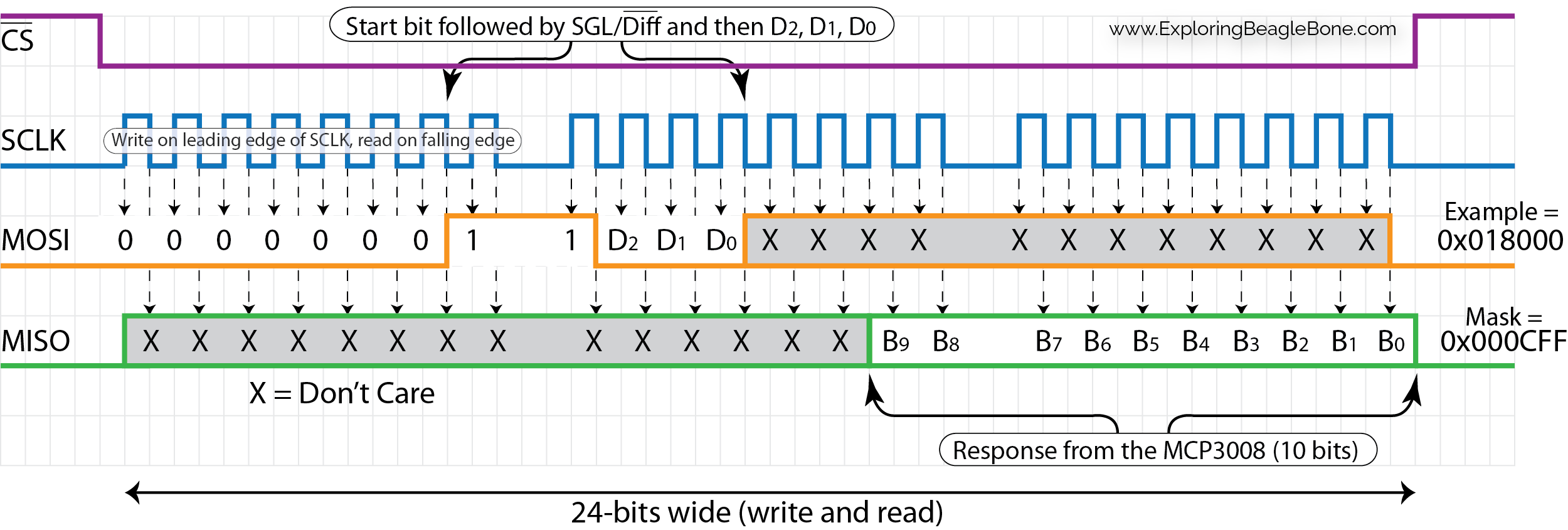 Figure 13.A3: The MCP3008 Data Communications Transaction
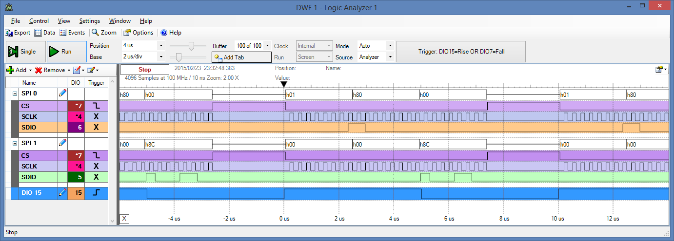 Figure 13.A4: Capture of a live data transaction between the PRUADC program and the MCP3008 IC Step 6. Once the pruadc application has executed, the sample data is transferred to the DDR external memory pool where it remains unless the program is executed again or the uio_pruss kernel module is unloaded/re-loaded. The mem2file program is a simple program that takes the data from memory and outputs it to the standard output so that it can be stored to a flat text-format file. The data is stored in DDR external memory with two bytes for each sample – the ADC program has a maximum of 16 bits of resolution per sample, which is sufficient for most low-cost ADCs and most applications. There is a script, plot (in Listing 13.A5), that captures the data from memory to a file and plots it to a PostScript file, which is further converted into a PDF format file. Listing 13.A5 The plot script
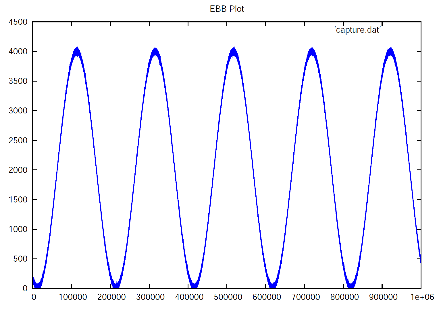
#!/bin/bash
echo "Capturing the first 2000 samples from the memory and dumping to capture.dat"
./mem2file 2000 > capture.dat

echo "Plotting the data to a PS file"
gnuplot <<_EOF_
set term postscript enhanced color
set output 'plot.ps'
set title 'EBB Plot'
plot 'capture.dat' with linespoints lc rgb 'blue'
_EOF_

echo "Converting the PS file to a PDF file"
ps2pdf plot.ps plot.pdf
It can be executed as follows:
root@beaglebone:~/exploringBB/chp13/adc# ./plot
Capturing the first 2000 samples from the memory and dumping to capture.dat
Plotting the data to a PS file
Converting the PS file to a PDF file
root@beaglebone:~/exploringBB/chp13/adc# ls plot*
plot  plot.pdf  plot.ps
root@beaglebone:~/exploringBB/chp13/adc#
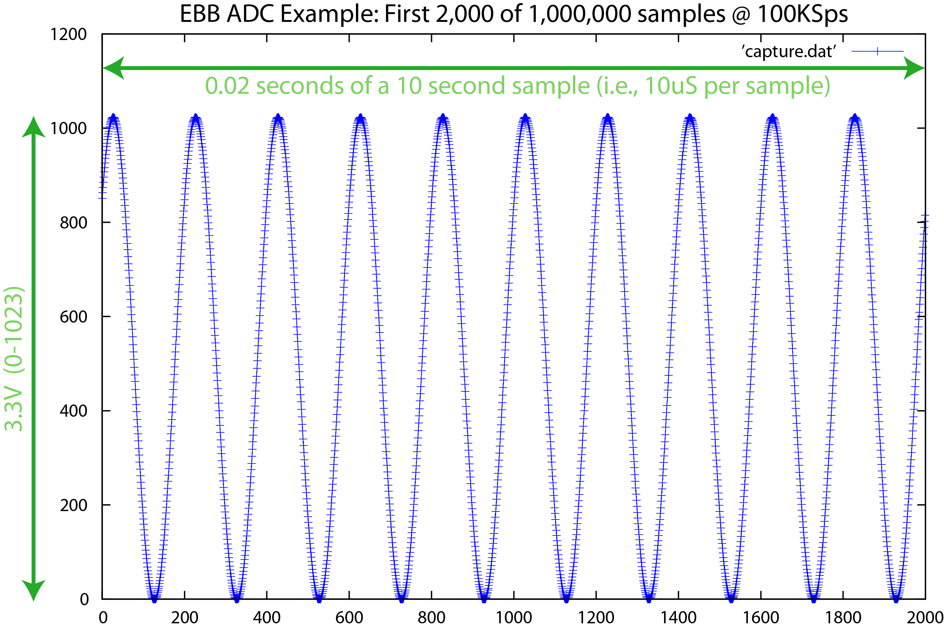
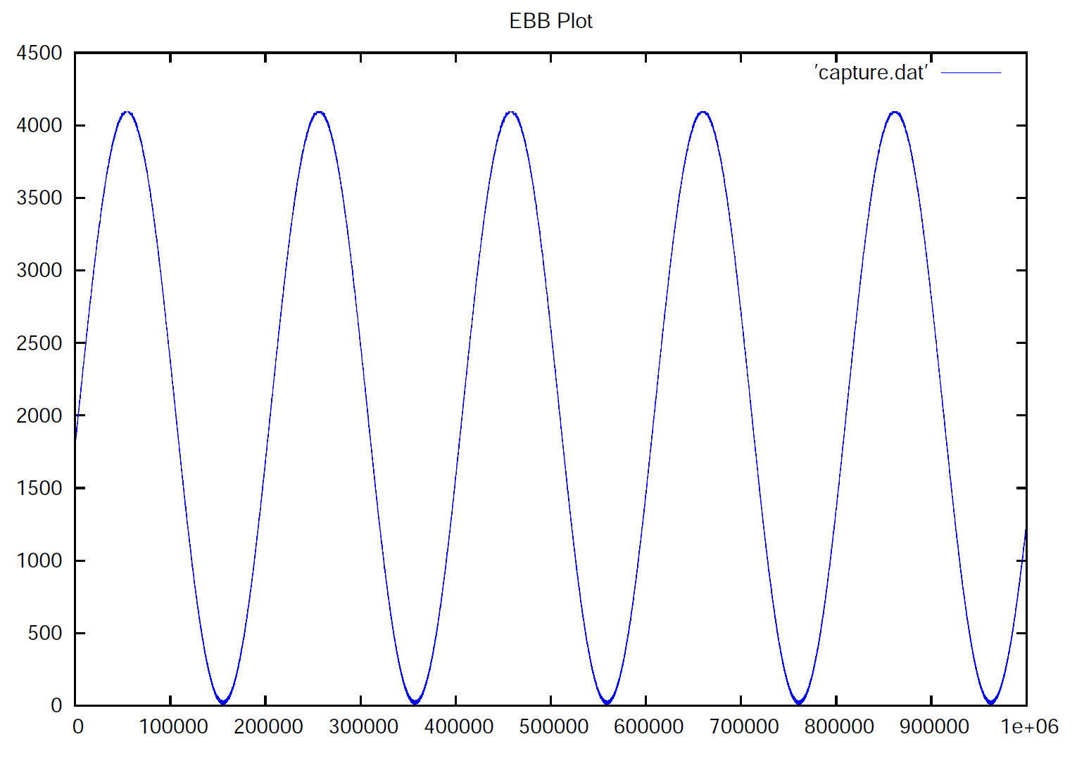
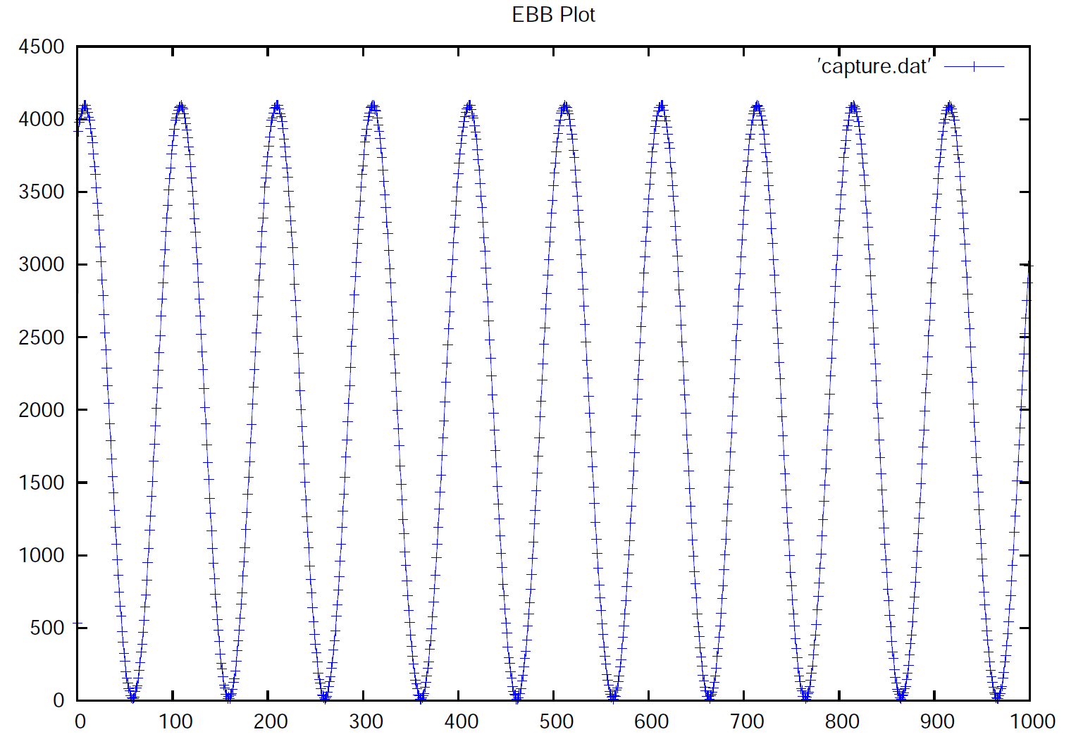
You can see some results from this application below in Figure 13.A5 and in the repository directory /chp13/adc/examples. In this example the Analog Discovery Waveform Generator applies a 500Hz sine wave (1.65V amplitude, +1.65V offset) to the Channel 0 input. Figure 13.A5 displays the sampled version of this wave — it is clear from this figure that the sample rate is very regular (albeit the sample frequency is slighly different than 100KSps). A PDF version of this figure is available here: plot_2000_samples_500Hz_input.
Figure 13.A5: An example output of the PRU SPI ADC application
Conclusions
While the structure for this application is slightly complex, it functions without any external oscillator for the sample clock and captures data at good sample rates considering the overall cost of the hardware configuration. The only limitation of the current implementation is that the sample size is limited by the available DDR memory pool size. That limitation can be addressed by streaming the data to the eMMC or to the network connection; however, it will required additional development work. If you use this work in your research, please cite this book.
The ADS7883 Single-Channel 12-bit ADC (1MSps max)
The MCP3008 can be used to sample up to 100kSps at 3.3V. For higher sampling rates there are alternative SPI ADC solutions available. Unfortunately, many are only available in surface-mount packages.
The ADS7883 (see the datasheet) is one such example. It is a 12-bit ADC that is capable of sampling at rates of up to 2MSps at 3.3V. Unfortunately it is only available in a 6-pin SOT23 package, which is a very small package for manual soldering. SOT to DIP form (0.1″) adapter boards are available, but even at that, it is a very small format IC. The ADS7883 is capable of sampling at 2MSps but the configuration that is presented in this discussion can only drive this IC at just over 1MSps approximately, as the software-controlled serial data clock frequency is approaching the limit of what is possible to generate using the PRU-ICSS.
The Circuit
The circuit configuration is illustrated in Figure 13.A6 and is very similar to the one that is used for the MCP3008 (in Figure 13.A1), with the exception that there is no requirement for the MOSI line, as there is no channel selection option on this IC. Rather, this IC samples and begins transmitting sample data as soon as the slave select (CS) line is pulled low by the BeagleBone. The serial clock line (CLK) is used for conversion and for synchronizing the serial data output.
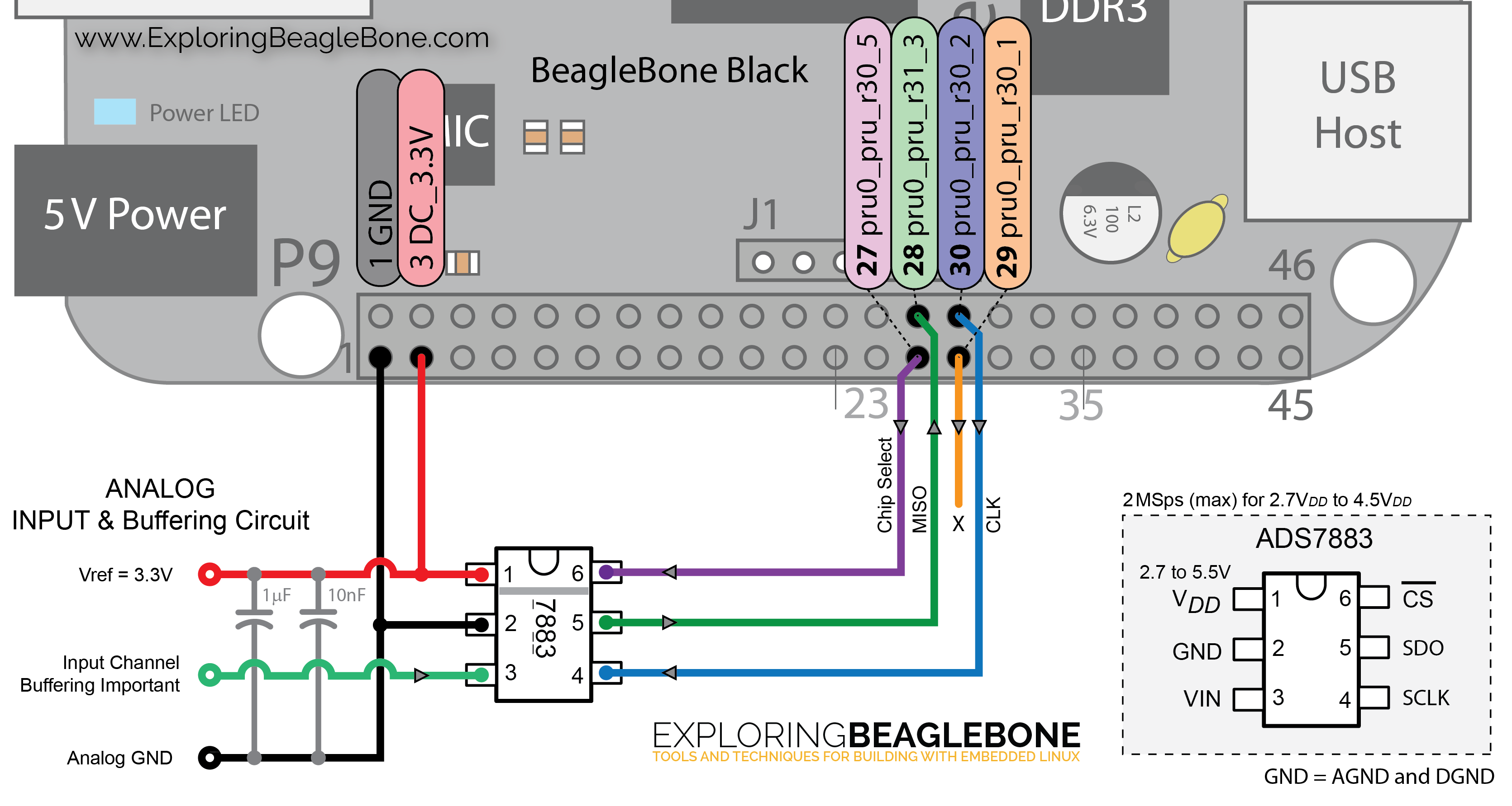
Figure 13.A6: The PRU-ADC circuit for the ADS7883 SPI ADC
- PRUADC_fixed_1MHz.p — this program can be used to sample at 1MHz (or a value close to that, which can be configured using the sample clock value in PRUADC.c). Replace the PRUADC.p program with this version and then use the build script.
- PRUADC_variable_rate.p — this program can be configured to sample at any frequency up to 500kSps. You can set the desired clock frequency in the PRUADC.c program.
All of the source code is available in the GitHub repository directory: /chp13/adc/ADS7883/
Using the Example Code
The device tree overlay can be loaded, and the DDR memory can be configured to store the sample data as follows. The sample capacity can be configured to contain up to 8MB of data — in this case 8,000,000 bytes (0x7A1200 HEX) are allocated, which is sufficient to capture 4 million 12-bit data samples (16-bits is the default data size for this code structure):
root@beaglebone:~# echo EBB-PRU-ADC > $SLOTS
root@beaglebone:~# cat $SLOTS | grep EBB
 7: ff:P-O-L Override Board Name,00A0,Override Manuf,EBB-PRU-ADC
root@beaglebone:~# rmmod uio_pruss
root@beaglebone:~# modprobe uio_pruss extram_pool_sz=0x7A1200
root@beaglebone:~# cd /sys/class/uio/uio0/maps/map1/
root@beaglebone:/sys/class/uio/uio0/maps/map1# cat addr
0x99000000
root@beaglebone:/sys/class/uio/uio0/maps/map1# cat size
0x7a1200
The programs will automatically detect the available memory space using sysfs and will capture data until this buffer is filled with 2-byte samples (containing 12-bits in this case). At a sample rate of 1MSps, this buffer will store four seconds of data.
root@beaglebone:~/exploringBB/chp13/adc/ADS7883# ls
EBB-PRU-ADC-00A0.dtbo  PRUADC.c		    PRUADC_variable_rate.p  README	 mem2file    plot.pdf
EBB-PRU-ADC.dts        PRUADC.p		    PRUClock.bin	    build	 mem2file.c  plot.ps
PRUADC.bin	       PRUADC_fixed_1MHz.p  PRUClock.p		    capture.dat  plot	     pruadc
root@beaglebone:~/exploringBB/chp13/adc/ADS7883# cp PRUADC_fixed_1MHz.p PRUADC.p
root@beaglebone:~/exploringBB/chp13/adc/ADS7883# ./build
Compiling the EBB-ADC overlay from .dts to .dtbo
...
root@beaglebone:~/exploringBB/chp13/adc/ADS7883# ./pruadc
The PRU clock state is set as period: 45 (0x2d) and state: 1
-> the PRUClock memory is mapped at the base address: 4a302000
-> the PRUClock on/off state is mapped at address: 4a310000
Sending the SPI Control Data: 0x0
The DDR External Memory pool has location: 0x99000000 and size: 0x7a1200 bytes
-> this space has capacity to store 4000000 16-bit samples (max)
...
root@beaglebone:~/exploringBB/chp13/adc/ADS7883# ./plot
Capturing the first 4,000,000 samples from the memory and dumping to capture.dat
Plotting the data to a PS file
Converting the PS file to a PDF file
The data can then be plotted using the plot script, which will take some time to plot 4 million sample points on the PostScript file and even more time to convert this into a PDF format on the BeagleBone. You can transfer this PDF file to your desktop machine using sftp so that it can be viewed. In addition, the number of samples to plot can be configured by modifying the first line of the plot script. Figure 13-A7 illustrates the capture of 4 million samples at 1MSps of a 1Hz sine wave (For this example, a 10nF capacitor was present on the Vin line/GND to reduce high-frequency impulse noise).
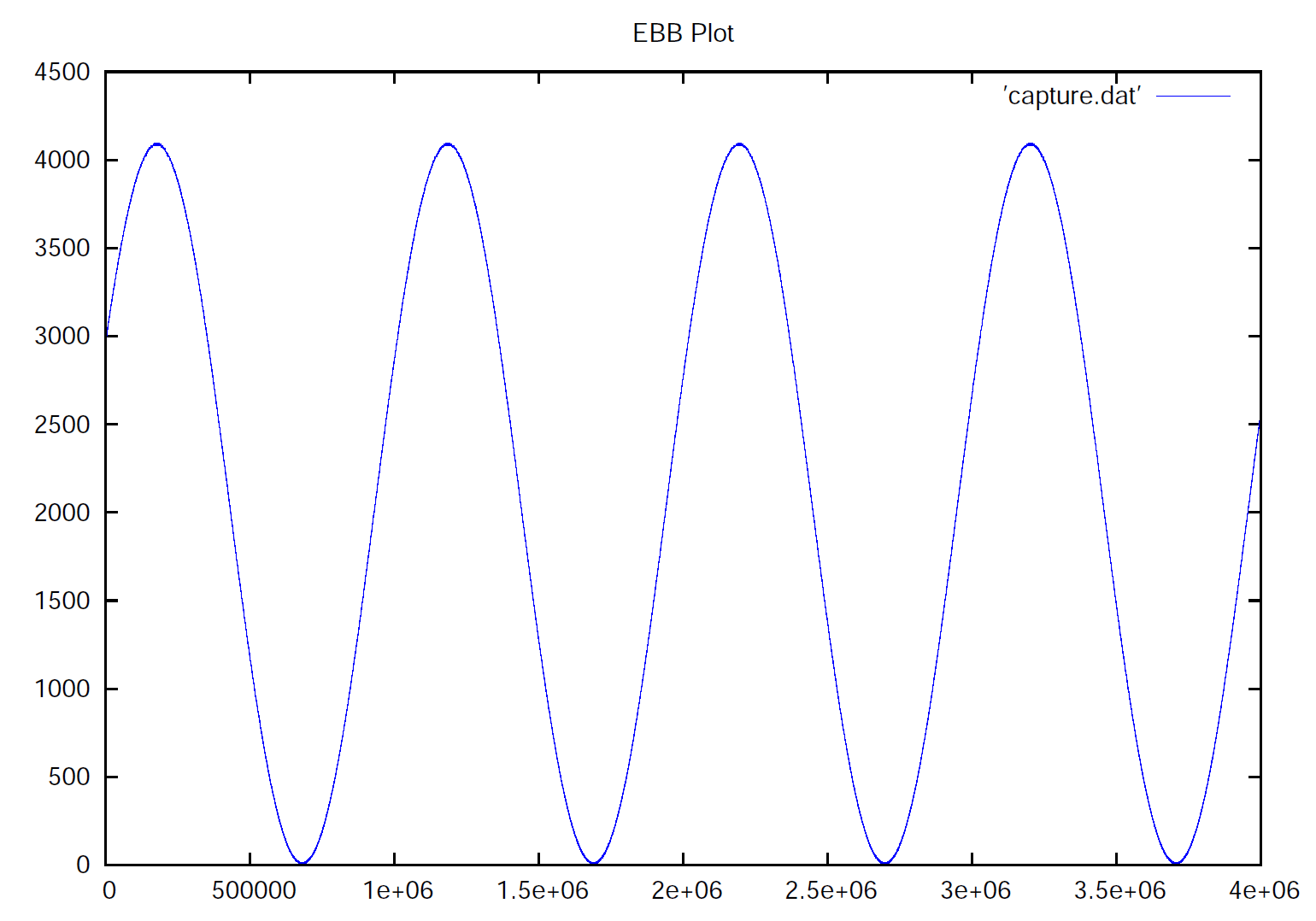
Figure 13-A7: Four million samples at 1MSps of a 1Hz input sine wave (click for larger image)
Data Communication
Figure 13-A8 captures a data exchange on the PRU pseudo-SPI bus as it is sampling at a rate of 1MSps. There is no data transmitted from the PRU to the ADS7883 on the MOSI line (orange), only from the ADS7883 on the MISO line (green). In this figure you can also see the sample clock that is generated using PRU1 on the bottom row of the figure. The rising edge of the sample clock (using the PRU shared memory address) causes the PRU0 to pull the CS line low (as in the MCP3008 example). That triggers the ADS7883 to take a sample. The data communications serial clock (SCLK) is toggled and the data is captured and transmitted on the rising edge of the data clock pulse (Note: I spent quite some time with this as the datasheet is not clear that the data is centered on the rising edge! Connecting the IC to a scope and using true SPI resolved this fact. Also, pay careful attention to the figures in the datasheet as GND and Vin are transposed in some of the figures).
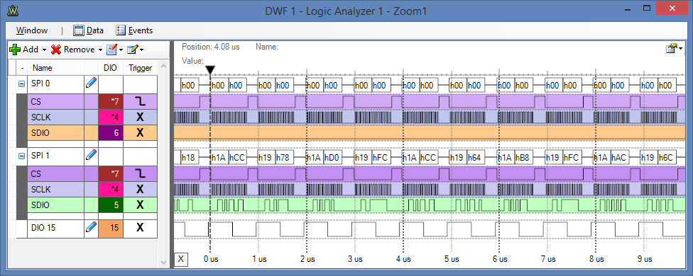
Figure 13-A8: The PRU SPI communications data transactions at 1MSps
You can see a single data sample transaction on the pseudo-SPI bus in Figure 13-A9 below. The data clock (CLK) uses the PRU instructions to transmit 16 samples in approximately 750nS (an effective rate of approximately 21.3MHz). Unfortunately, this is getting close to the physical limit of the PRUs, as each PRU instruction takes exactly 5ns, but the code to receive and capture the data must be intermixed with the code to toggle the data clock signal. The only way to achieve much faster sample rates would be to use a parallel ADC, which would itself create problems with enhanced GPIO availability. The rate could be pushed to approx. 1.5MSps with this application, but I don’t think that a much higher sample rates are possible with my code structure — perhaps 2MSps at most!
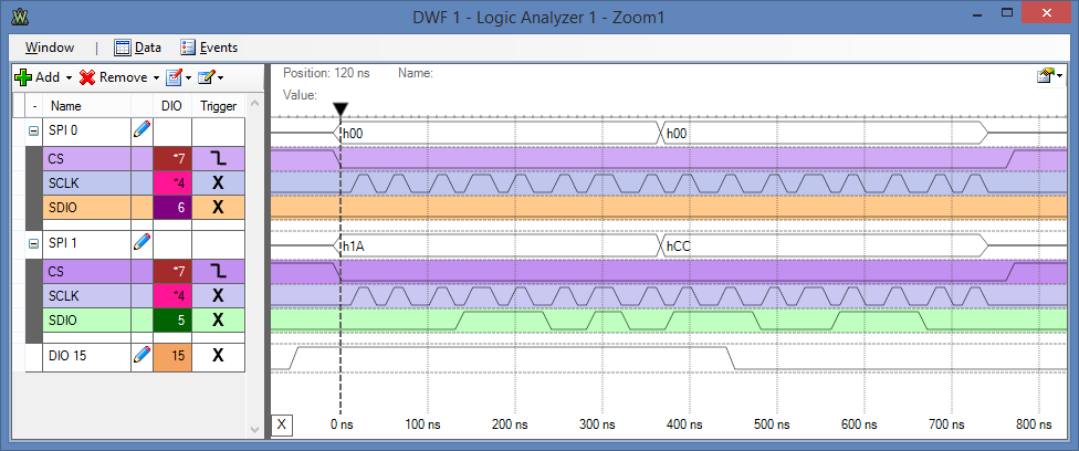
Figure 13-A9: The PRU SPI communications data transaction at 1MSps (1 data transaction)
In this example, the data that is transmitted in Figure 13-A9 on the MISO line (green) is 0x1ACC, which is 0001 1010 1100 1100 in binary. For this IC, the first two leading bits are always zero, as are the last two bits, giving: 0110 1011 0011, the 12-bit data sample which is 0x6B3 or 1715/4095 in decimal. The PRU code shifts the resulting sample right by two positions and ORs it with 0x00000FFF to ensure that the remainder of the data sample value is ignored. It then stores the sample data in external DDR memory.
Results
The circuit can be tested by applying input signals and measuring the resulting sampled data. The datasheet for the ADS7883 recommends the use of decoupling capacitors on the supply (See Figure 25 in the datasheet — note that Vin and GND are transposed) to reduce the sampling noise, and they are certainly necessary. Additionally, the datasheet recommends the use of buffering on the supply voltage (see Figure 27 in the datasheet) which is likely necessary if you are using the BeagleBone supply. With decoupling capacitors alone there is an unusual noise response on the input, only when the device is sampling. This can be observed in Figure 13.A10.
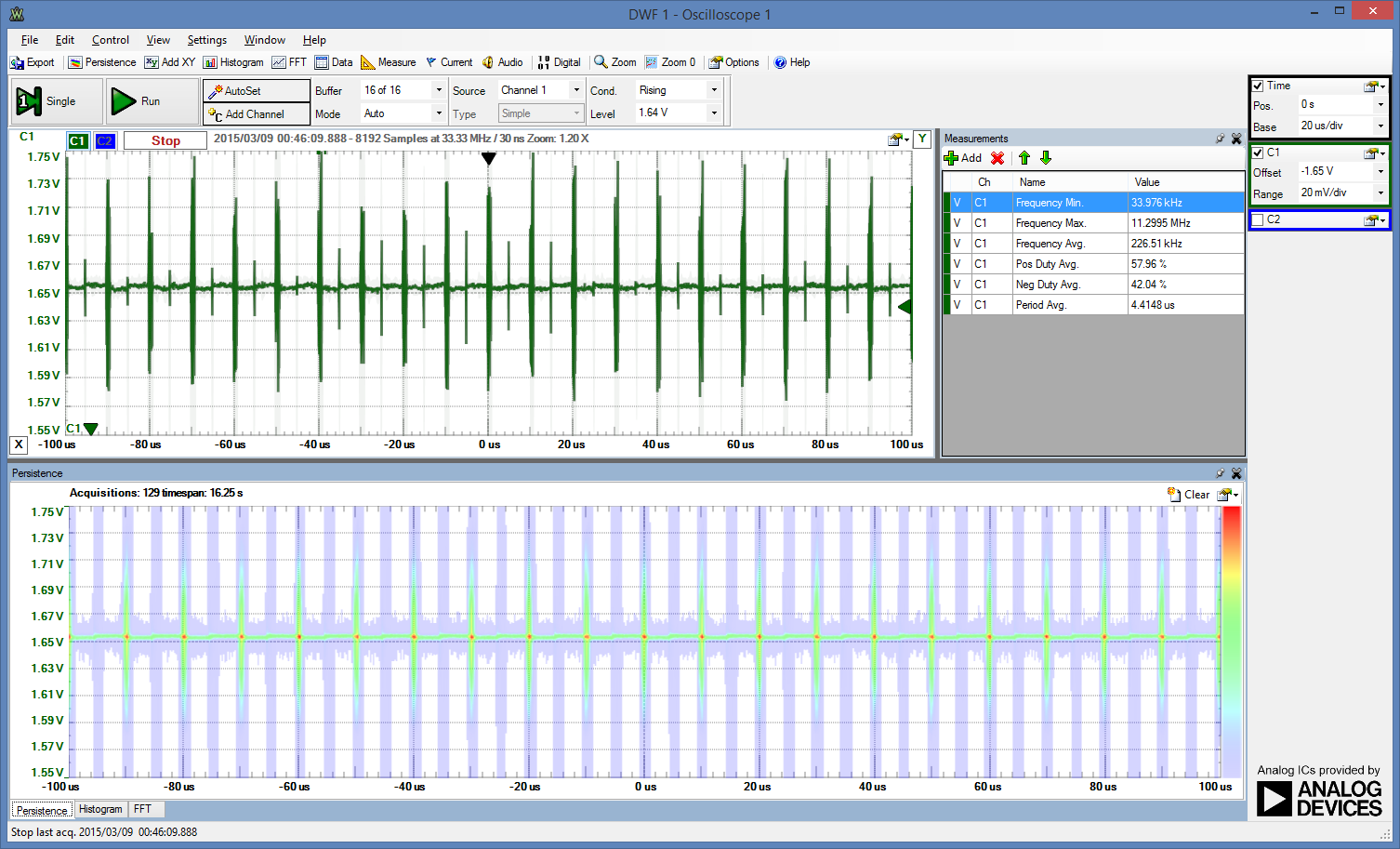
Figure 13.A10: Example signal noise that is present on the ADS7883 Vin input during sampling
The noise occurs every 10uS but is impulsive in nature. To counter this noise a small capacitor (e.g., 10nF — please choose this to suit the impedance of your application sensor type) can be placed between Vin and GND. You can choose this capacitor to suit the sampling rate required for your application. At 1MSps the Nyquist frequency is 500kHz so a high-frequency low-pass filter on the input can greatly improve the signal quality. The shared analog/digital GNDand Vref/Vcc likely reduces the overall IC cost, but it appears to affect the sample quality.
 (a) 1 million samples at 1MSps — 5Hz input with noise (no Vin cap)
(b) 1 million samples at 1MSps — 5Hz input with Vin cap (10nF)
(c) first 1,000 of 1 million samples at 1MSps — 10kHz input with Vin cap (10nF)
(d) first 1,000 of 1 million samples at 1MSps — 100kHz input with Vin cap (10nF)
Figure 13.A11: Sample results with input signals of different frequences
The results in Figure 13.A11 illustrate some example outputs from this application. The first sample (a) illustrates the impact of the impulse noise on the captured signal. The second sample (b) illustrates the impact of adding a 10nF capacitor across Vin/GND for this example. In (c), only the first 1,000 samples are displayed of the signal which was sampled at 1MSps — you can see that the sampling rate is regular. Finally, in (d) the first 1,000 samples of a 100kHz input signal is displayed. At this rate there are only 10 samples for each period of the input signal, leading to the aliasing pattern, the regularity of which indicates that there is very low jitter.
It may be necessary for you to rebuild the uio_pruss kernel module for your application. For example, you could alter the default external memory allocation so that you would not have to remove the module and reload it with the use of an argument that defines the size of memory to allocate.
The first step is to ensure that your BBB is set up to compile kernel modules. To do that you need to install the Linux-headers for your exact distribution. You can find them at Robert Nelson’s website — for example, at: http://rcn-ee.net/deb/precise-armhf/. Use uname -a to determine your exact distribution, and then download and install those Linux-headers on your BBB using the website — for example:
molloyd@beaglebone:~/tmp$ uname -a
Linux beaglebone 3.8.13-bone70 #1 SMP Fri Jan 23 02:15:42 UTC 2015 armv7l GNU/Linux

molloyd@beaglebone:~/tmp$ wget http://rcn-ee.net/deb/precise-armhf/v3.8.13-bone70/linux-headers-3.8.13-bone70_1precise_armhf.deb
…
100%[=========================================================>] 8,451,080   2.52M/s   in 3.2s
2015-03-17 22:35:45 (2.52 MB/s) - `linux-headers-3.8.13-bone70_1precise_armhf.deb' saved [8451080/8451080]

molloyd@beaglebone:~/tmp$ sudo dpkg -i ./linux-headers-3.8.13-bone70_1precise_armhf.deb
Selecting previously unselected package linux-headers-3.8.13-bone70.
...
molloyd@beaglebone:~/tmp$ cd /usr/src/linux-headers-3.8.13-bone70/
molloyd@beaglebone:/usr/src/linux-headers-3.8.13-bone70$ ls
Documentation  Module.symvers  crypto    fs       ipc     mm       scripts   tools
Kconfig        arch            drivers   include  kernel  net      security  usr
Makefile       block           firmware  init     lib     samples  sound     virt
Under the 3.8.13 bone50 BBB Debian distribution you may have to create an empty file timex.h (i.e., touch timex.h) in the directory /usr/src/linux-headers-3.8.13-bone50/arch/arm/include/mach.
Then, using the source code in the GitHub repository you can alter the uio_pruss.c file to suit your application. In this source code example the default external memory size is set for 512K, rather than 256K:
molloyd@beaglebone:~/tmp$ cd ~/exploringBB/chp13/kernel/3.8.13_bone70/

molloyd@beaglebone:~/exploringBB/chp13/kernel/3.8.13_bone70$ ls
Makefile  Module.symvers  modules.order  uio_pruss.c  uio_pruss.ko  uio_pruss.mod.c  uio_pruss.mod.o  uio_pruss.o

molloyd@beaglebone:~/exploringBB/chp13/kernel/3.8.13_bone70$ make
make -C /lib/modules/3.8.13-bone70/build/ M=/home/molloyd/exploringBB/chp13/kernel/3.8.13_bone70 modules
make[1]: Entering directory `/usr/src/linux-headers-3.8.13-bone70'
  CC [M]  /home/molloyd/exploringBB/chp13/kernel/3.8.13_bone70/uio_pruss.o
Building modules, stage 2.
  MODPOST 1 modules
  CC      /home/molloyd/exploringBB/chp13/kernel/3.8.13_bone70/uio_pruss.mod.o
  LD [M]  /home/molloyd/exploringBB/chp13/kernel/3.8.13_bone70/uio_pruss.ko
make[1]: Leaving directory `/usr/src/linux-headers-3.8.13-bone70'
Once the module is built, it will appear as uio_pruss.ko in the current directory. You can load this module and test it as follows:
molloyd@beaglebone:~/exploringBB/chp13/kernel/3.8.13_bone70$ sudo insmod ./uio_pruss.ko
molloyd@beaglebone:~/exploringBB/chp13/kernel/3.8.13_bone70$ lsmod
Module                  Size  Used by
uio_pruss               4066  0
…
molloyd@beaglebone:~/exploringBB/chp13/kernel/3.8.13_bone70$ cd /sys/class/uio/uio0/maps/map1
molloyd@beaglebone:/sys/class/uio/uio0/maps/map1$ cat addr
0x9e680000
molloyd@beaglebone:/sys/class/uio/uio0/maps/map1$ cat size
0x80000
You can see that the uio_pruss kernel module external memory now has a default size of 0x80000 — 524,288 bytes, which is 512Kbytes (note the big K) as specified in the new uio_pruss.c example code. To replace the default module, copy the uio_pruss.ko file to the bottom location below (remembering to make a backup of the original):
root@beaglebone:/# find -name uio_pruss.ko
./home/molloyd/exploringBB/chp13/kernel/3.8.13_bone50/uio_pruss.ko
./home/molloyd/exploringBB/chp13/kernel/3.8.13_bone70/uio_pruss.ko
./lib/modules/3.8.13-bone70/kernel/drivers/uio/uio_pruss.ko
PRU-based Clock Signal Generators
[Added Feb, 2015] In this example a real-time variable-frequency clock is built using the PRU-ICSS. In Chapter 13, a PWM example is developed over a number of sections and the implementation in this discussion is relatively straightforward in comparison to that example. However, a PRU clock is a useful addition to the range of PRU examples available, and it is further used to explain how to develop a PRU program that can be executed “permanently” on a PRU, while remaining configurable from Linux userspace. The circuit required for this example is very straightforward. It uses the same DTD that is described in the chapter in order to output the clock signal on pin P9_27, which is pru0_pru_r30_5. The HDMI cape has been disabled, as discussed at the beginning of the chapter. In all examples within this section the Analog Discovery Oscilloscope is connected to P9_27 (and GND — e.g., pin P9_2) in order to measure the output response.
A Fixed-Frequency PRU-based Clock
It is useful to begin with a straightforward example before continuing to the variable-frequency clock example. In fact, if all you require is a fixed-frequency clock then the following example will suffice. The first code example demonstrates how a clock signal how a clock signal, which has a 50% duty cycle, can be configured by hard-coding a delay into the PRU program code. Remember that with the PRU-ICSS, each instruction takes exactly 5ns to execute. Using this fact the following program outputs a 20MHz square wave clock signal on P9_27. You must load the PRU overlay EBB-PRU in advance, and can execute the program using the following steps:
root@beaglebone:~/exploringBB/chp13/overlay# cp EBB-PRU-Example-00A0.dtbo /lib/firmware/
root@beaglebone:~/exploringBB/chp13/overlay# cd /lib/firmware/
root@beaglebone:/lib/firmware# ls EBB*
EBB-PRU-Example-00A0.dtbo
root@beaglebone:/lib/firmware# echo EBB-PRU-Example > $SLOTS
root@beaglebone:/lib/firmware# cat $SLOTS
 0: 54:PF---
 1: 55:PF---
 2: 56:PF---
 3: 57:PF---
 4: ff:P-O-L Bone-LT-eMMC-2G,00A0,Texas Instrument,BB-BONE-EMMC-2G
 5: ff:P-O-- Bone-Black-HDMI,00A0,Texas Instrument,BB-BONELT-HDMI
 6: ff:P-O-- Bone-Black-HDMIN,00A0,Texas Instrument,BB-BONELT-HDMIN
 7: ff:P-O-L Override Board Name,00A0,Override Manuf,EBB-PRU-Example
root@beaglebone:/lib/firmware# cd ~/exploringBB/chp13/fixedPRUClock/
root@beaglebone:~/exploringBB/chp13/fixedPRUClock# ls
FixedPRUClock.bin  FixedPRUClock.c  FixedPRUClock.p  build  fixedclock
root@beaglebone:~/exploringBB/chp13/fixedPRUClock# ./build
PRU Assembler Version 0.84
Copyright (C) 2005-2013 by Texas Instruments Inc.
Pass 2 : 0 Error(s), 0 Warning(s)
Writing Code Image of 12 word(s)
root@beaglebone:~/exploringBB/chp13/fixedPRUClock# ./fixedclock
EBB fixed-frequency clock PRU program now running
root@beaglebone:~/exploringBB/chp13/fixedPRUClock#
The source code for this example follows below. The full project is available in the /chp13/fixedPRUClock directory of the GitHub repository, but the important code is presented here along with comments describing its operation. Please note that there was a duplicated instruction required to ensure that the output clock signal has a 50% duty cycle (i.e., on for 50% of the time and off for 50% of the time).
FixedPRUClock.p
// PRU program to provide a fixed-frequency clock on P9_27 (pru0_pru_r30_5). This
// program can be executed on either PRU0 or PRU1, but will have to be altered if
// you wish to change the clock to output on a different pin. Memory controlled:
// This program was writen by Derek Molloy to align with the content of the book
// Exploring BeagleBone

.origin 0                        // start of program in PRU memory
.entrypoint START                // program entry point (for a debugger)

#define	DELAY   498  		 // choose the delay value to suit the frequency required
				 // 1 gives a 20MHz clock signal, increase from there
START:
	MOV	r1, DELAY	 // load the DELAY value into r1

MAINLOOP:
	CLR	r30.t5		// set the clock to be low
	CLR	r30.t5		// set the clock to be low -- to balance the duty cycle
	MOV	r0, r1		// load the delay r1 into temp r0 (50% duty cycle)

DELAYOFF:
	SUB	r0, r0, 1	// decrement the counter by 1 and loop (next line)
	QBNE	DELAYOFF, r0, 0	// loop until the delay has expired (equals 0)
	SET	r30.t5		// set the clock to be high
	MOV	r0, r1		// re-load the delay r1 into temporary r0

DELAYON:
	SUB	r0, r0, 1	// decrement the counter by 1 and loop (next line)
	QBNE	DELAYON, r0, 0	// loop until the delay has expired (equals 0)

	QBA	MAINLOOP	// start again, so the program will not exit
END:
	HALT			// halt the pru program -- never reached
FixedPRUClock.c
/** Program to load a PRU program that flashes an LED until a button is
*   pressed. By Derek Molloy, for the book Exploring BeagleBone
*   based on the example code at:
*   http://processors.wiki.ti.com/index.php/PRU_Linux_Application_Loader_API_Guide
*/

#include <stdio.h>
#include <stdlib.h>
#include <prussdrv.h>
#include <pruss_intc_mapping.h>

#define PRU_NUM	0   // using PRU0 for these examples

int main (void)
{
   if(getuid()!=0){
      printf("You must run this program as root. Exiting.\n");
      exit(EXIT_FAILURE);
   }
   // Initialize structure used by prussdrv_pruintc_intc
   // PRUSS_INTC_INITDATA is found in pruss_intc_mapping.h
   tpruss_intc_initdata pruss_intc_initdata = PRUSS_INTC_INITDATA;

   // Allocate and initialize memory
   prussdrv_init ();
   prussdrv_open (PRU_EVTOUT_0);

   // Map PRU's interrupts
   prussdrv_pruintc_init(&pruss_intc_initdata);

   // Load and execute the PRU program on the PRU
   prussdrv_exec_program (PRU_NUM, "./FixedPRUClock.bin");
   printf("EBB fixed-frequency clock PRU program now running\n");

   prussdrv_exit ();
   return EXIT_SUCCESS;
}
EBB-PRU-Example.dts
/* Device Tree Overlay for enabling the pins that are used in Chapter 13
* This overlay is based on the BB-PRU-01 overlay
* Written by Derek Molloy for the book "Exploring BeagleBone: Tools and
* Techniques for Building with Embedded Linux" by John Wiley & Sons, 2014
* ISBN 9781118935125. Please see the file README.md in the repository root
* directory for copyright and GNU GPLv3 license information.
*/
/dts-v1/;
/plugin/;

/ {
   compatible = "ti,beaglebone", "ti,beaglebone-black";

   part-number = "EBB-PRU-Example";
   version = "00A0";

   /* This overlay uses the following resources */
   exclusive-use =
         "P9.11", "P9.13", "P9.27", "P9.28", "pru0";

   fragment@0 {
      target = <&am33xx_pinmux>;
      __overlay__ {

         gpio_pins: pinmux_gpio_pins {         // The GPIO pins
            pinctrl-single,pins = <
               0x070 0x07  // P9_11 MODE7 | OUTPUT | GPIO pull-down
               0x074 0x27  // P9_13 MODE7 | INPUT | GPIO pull-down
            >;
         };

         pru_pru_pins: pinmux_pru_pru_pins {   // The PRU pin modes
            pinctrl-single,pins = <
               0x1a4 0x05  // P9_27 pr1_pru0_pru_r30_5, MODE5 | OUTPUT | PRU
               0x19c 0x26  // P9_28 pr1_pru0_pru_r31_3, MODE6 | INPUT | PRU
            >;
         };
      };
   };

   fragment@1 {         // Enable the PRUSS
      target = <&pruss>;
      __overlay__ {
         status = "okay";
         pinctrl-names = "default";
         pinctrl-0 = <&pru_pru_pins>;
      };
   };

   fragment@2 {         // Enable the GPIOs
      target = <&ocp>;
      __overlay__ {
         gpio_helper {
            compatible = "gpio-of-helper";
            status = "okay";
            pinctrl-names = "default";
            pinctrl-0 = <&gpio_pins>;
         };
      };
   };
};
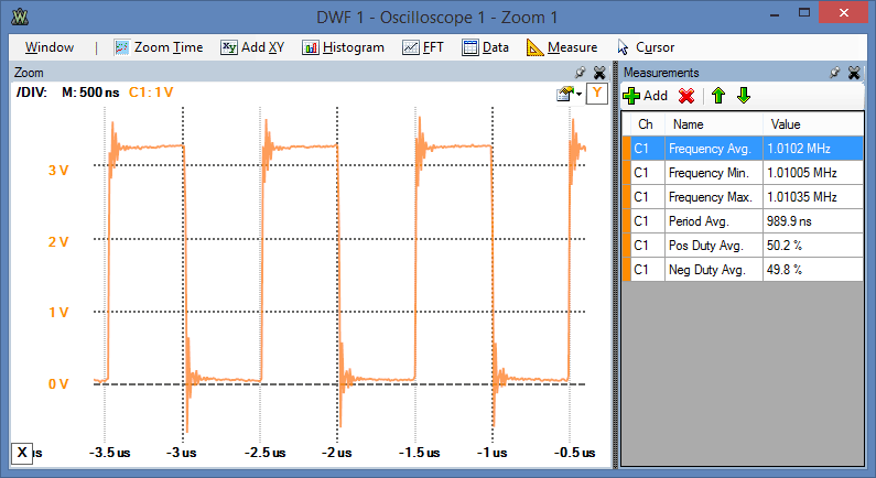
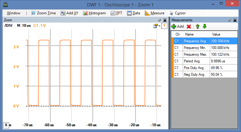 Figure 13.B1: Clock signal on P9_27 (a) 1MHz signal using a hard-coded delay value of 48 and (b) 100kHz using a hard-coded delay value of 498 utilize both PRUs. One important feature of these signals is that they do not suffer from jitter as they are executing independent of the load that the embedded Linux processor is currently undertaking. The downside is that (without careful programming) you can only have two such signals, each of which is occupying a valuable PRU. An alternative configuration is to use an external crystal, but that is not necessary if your embedded application does not utilize both PRUs.
A Variable-Frequency PRU-based Clock
The example in the last section is improved in this section so that the frequency of the clock can be adjusted from the Linux userspace, even while the PRU program is running. For this example, the devmem2 application is utilized again; however, a C/C++ program could be written in its place. Once the PRU overlay is loaded and the oscilloscope is attached to P9_27 as before, the program can be executed as follows:
root@beaglebone:~/exploringBB/chp13/PRUClock# ./pruclock
The clock state is set as period: 47 (0x2f) and state: 1
This is mapped at the base address: 4a300000
EBB Clock PRU program now running (47)
The program outputs a 1MHz clock signal by default. The program also identifies the PRU memory base address as above (at 0x4a300000) at which the period value can be placed (in 4 bytes). To output a clock signal at 1MHz a value of 47 is used, which is 0x2f in hexadecimal. The devmem2 program can be used to query this address, which will result in the following output:
root@beaglebone:~/exploringBB/chp13/PRUClock# ../devmem2/devmem2 0x4a300000
/dev/mem opened.
Memory mapped at address 0xb6f33000.
Value at address 0x4A300000 (0xb6f33000): 0x2F
The same devmem2 program can be used to write a new value (word in this case, using w) to the address — in this case 497, which is 0x1F1 in hexadecimal. This corresponds to an output clock signal frequency of approximately 100kHz:
root@beaglebone:~/exploringBB/chp13/PRUClock# ../devmem2/devmem2 0x4a300000 w 0x1F1
/dev/mem opened.
Memory mapped at address 0xb6f4c000.
Value at address 0x4A300000 (0xb6f4c000): 0x2F
Written 0x1F1; readback 0x1F1
However, the output will not be updated until the value in the subsequent memory address 0x4a300004 is update to a value of 3 (i.e., both LSBs are set to 1). It has been programmed this way to ensure that it is possible to update the clock frequency (see the PRU code):
root@beaglebone:~/exploringBB/chp13/PRUClock# ../devmem2/devmem2 0x4a300004 b 3
/dev/mem opened.
Memory mapped at address 0xb6fde000.
Value at address 0x4A300004 (0xb6fde004): 0x1
Written 0x3; readback 0x3
At this point the clock output frequency will update to 100kHz and the PRU program will set the value in the subsequent memory address to 1 (i.e., unsetting the second-most LSB — the value thus changes from 3 decimal to 1 decimal).
root@beaglebone:~/exploringBB/chp13/PRUClock# ../devmem2/devmem2 0x4a300004
/dev/mem opened.
Memory mapped at address 0xb6fab000.
Value at address 0x4A300004 (0xb6fab004): 0x1
root@beaglebone:~/exploringBB/chp13/PRUClock#
The clock will continue to output the clock signal until the value is updated again or the BeagleBone is rebooted. The full project is available in the /chp13/PRUClock directory of the GitHub repository, but the important code is presented here along with comments describing its operation.
PRUClock.p
// PRU program to provide a variable frequency clock on P9_27 (pru0_pru_r30_5)
// that is controlled from Linux userspace by setting the PRU memory state. This
// program can be executed on either PRU0 or PRU1, but will have to be altered if
// you wish to change the clock to output on a different pin. Memory controlled:
// - The delay is set in memory address 0x00000000 (4 bytes)
// - The counter can be turned on and off by setting the LSB 0x00000004 (4 bytes)
//   to 1 (on) or 0 (off)
// - The delay value can be updated by setting the second most LSB to 1 (it will
//   immediately return to 0)
// This program was writen by Derek Molloy to align with the content of the book
// Exploring BeagleBone

.origin 0                        // start of program in PRU memory
.entrypoint START                // program entry point (for a debugger)

START:	                         // load the clock period value into r2
	MOV	r1, 0x00000000	 // load the base address into r1
	LBBO	r2, r1, 0, 4	 // the clock delay is now loaded into r2. 4 bytes.
	QBA	ENDOFLOOP	 // move to comparison -- avoids duplicating code

MAINLOOP:
	CLR	r30.t5           // set the clock to be low
	MOV	r0, r2		 // load the delay r2 into temp r0 (50% duty cycle)
	ADD	r0, r0, 1	 // balance duty cycle by looping 1 extra time on low

DELAYOFF:
	SUB	r0, r0, 1	 // decrement the counter by 1 and loop (next line)
	QBNE	DELAYOFF, r0, 0  // loop until the delay has expired (equals 0)
				 // next code order used to help keep 50% duty cycle
	MOV	r0, r2           // re-load the delay r2 into temporary r0
	SET	r30.t5		 // set the clock to be high

DELAYON:
	SUB	r0, r0, 1	 // decrement the counter by 1 and loop (next line)
	QBNE	DELAYON, r0, 0   // loop until the delay has expired (equals 0)

ENDOFLOOP:                       // is the clock running?
	LBBO	r3, r1, 4, 4	 // loaded in the state into r3 -- is running? 4 bytes.
	QBBS	RESETCLK, r3.t1	 // If r3 bit 1 is high then reload the clock period
	QBBS	MAINLOOP, r3.t0  // If r3 bit 0 is high then the clock is running
	QBA	ENDOFLOOP        // otherwise loop without toggling the clock

RESETCLK:			 // clear the r3.t1 bit and write back to memory
	CLR	r3, r3.t1	 // i.e., clear the reload clock flag
	SBBO	r3, r1, 4, 4     // write that value back into memory
	QBA	START            // go back to the start of the program

END:				 // program will not exit
	HALT                     // halt the pru program -- never reached
PRUClock.c
/** Program to load a PRU program that flashes an LED until a button is
*   pressed. By Derek Molloy, for the book Exploring BeagleBone
*   based on the example code at:
*   http://processors.wiki.ti.com/index.php/PRU_Linux_Application_Loader_API_Guide
*/

#include <stdio.h>
#include <stdlib.h>
#include <prussdrv.h>
#include <pruss_intc_mapping.h>

#define PRU_NUM	   0   // using PRU0 for these examples
#define MMAP_LOC   "/sys/class/uio/uio0/maps/map0/"

enum FREQUENCY {    // measured and calibrated, but can be calculated
	FREQ_12_5MHz =  1,
	FREQ_6_25MHz =  5,
	FREQ_5MHz    =  7,
	FREQ_3_85MHz = 10,
	FREQ_1MHz   =  47,
	FREQ_500kHz =  97,
	FREQ_250kHz = 247,
	FREQ_100kHz = 497,
	FREQ_25kHz = 1997,
	FREQ_10kHz = 4997,
	FREQ_5kHz =  9997,
	FREQ_2kHz = 24997,
	FREQ_1kHz = 49997
};

enum CONTROL {
	PAUSED = 0,
	RUNNING = 1,
	UPDATE = 3
};

unsigned int readFileValue(char filename[]){
   FILE* fp;
   unsigned int value = 0;
   fp = fopen(filename, "rt");
   fscanf(fp, "%x", &value);
   fclose(fp);
   return value;
}

int main (void)
{
   if(getuid()!=0){
      printf("You must run this program as root. Exiting.\n");
      exit(EXIT_FAILURE);
   }
   // Initialize structure used by prussdrv_pruintc_intc
   // PRUSS_INTC_INITDATA is found in pruss_intc_mapping.h
   tpruss_intc_initdata pruss_intc_initdata = PRUSS_INTC_INITDATA;

   // Read in the location and address of the shared memory. This value changes
   // each time a new block of memory is allocated.
   unsigned int values[2];
   values[0] = FREQ_1MHz;
   values[1] = RUNNING;
   printf("The clock state is set as period: %d (0x%x) and state: %d\n", values[0], values[0], values[1]);
   printf("This is mapped at the base address: %x\n", readFileValue(MMAP_LOC "addr"));

   // Allocate and initialize memory
   prussdrv_init ();
   prussdrv_open (PRU_EVTOUT_0);

   // Write the address and size into PRU0 Data RAM0. You can edit the value to
   // PRUSS0_PRU1_DATARAM if you wish to write to PRU1
   prussdrv_pru_write_memory(PRUSS0_PRU0_DATARAM, 0, values, 8);

   // Map PRU's interrupts
   prussdrv_pruintc_init(&pruss_intc_initdata);

   // Load and execute the PRU program on the PRU
   prussdrv_exec_program (PRU_NUM, "./PRUClock.bin");
   printf("EBB Clock PRU program now running (%d)\n", values[0]);

   prussdrv_exit ();
   return EXIT_SUCCESS;
}
EBB-PRU-Example.dts
/* Device Tree Overlay for enabling the pins that are used in Chapter 13
* This overlay is based on the BB-PRU-01 overlay
* Written by Derek Molloy for the book "Exploring BeagleBone: Tools and
* Techniques for Building with Embedded Linux" by John Wiley & Sons, 2014
* ISBN 9781118935125. Please see the file README.md in the repository root
* directory for copyright and GNU GPLv3 license information.
*/
/dts-v1/;
/plugin/;

/ {
   compatible = "ti,beaglebone", "ti,beaglebone-black";

   part-number = "EBB-PRU-Example";
   version = "00A0";

   /* This overlay uses the following resources */
   exclusive-use =
         "P9.11", "P9.13", "P9.27", "P9.28", "pru0";

   fragment@0 {
      target = <&am33xx_pinmux>;
      __overlay__ {

         gpio_pins: pinmux_gpio_pins {         // The GPIO pins
            pinctrl-single,pins = <
               0x070 0x07  // P9_11 MODE7 | OUTPUT | GPIO pull-down
               0x074 0x27  // P9_13 MODE7 | INPUT | GPIO pull-down
            >;
         };

         pru_pru_pins: pinmux_pru_pru_pins {   // The PRU pin modes
            pinctrl-single,pins = <
               0x1a4 0x05  // P9_27 pr1_pru0_pru_r30_5, MODE5 | OUTPUT | PRU
               0x19c 0x26  // P9_28 pr1_pru0_pru_r31_3, MODE6 | INPUT | PRU
            >;
         };
      };
   };

   fragment@1 {         // Enable the PRUSS
      target = <&pruss>;
      __overlay__ {
         status = "okay";
         pinctrl-names = "default";
         pinctrl-0 = <&pru_pru_pins>;
      };
   };

   fragment@2 {         // Enable the GPIOs
      target = <&ocp>;
      __overlay__ {
         gpio_helper {
            compatible = "gpio-of-helper";
            status = "okay";
            pinctrl-names = "default";
            pinctrl-0 = <&gpio_pins>;
         };
      };
   };
};
External Resources
Important Documents
External Web Sites
The AM335x Technical Reference Manual (TRM)
The AM335x PRU-ICSS Reference Guide (289 pages)
(click “view raw”)
- The Texas Instruments PRU Wiki: tiny.cc/ebb1308
- The PRU Linux Application Loader API Guide: tiny.cc/ebb1309
- The PRU Debugger User Guide: tiny.cc/ebb1310
Errata
Second Edition
- None so far
First Edition
- On page 510 there is an error of omission in Listing 13-1. The code in the GitHub repository (and presented on this page) is complete. The listing in the book should be read as a code segment and not a complete listing. The omission is “fragment@0 { target = <&am33xx_pinmux>; __overlay__ {” after the line that begins “exclusive-use”.
- On page 524 there is a confusing constant name in the code example — GPIO_DATAOUT should more correctly be labelled GPIO_DATAIN. The source code example has been adjusted.
- On page 527 the sentence that ends “low-pass filtered output” in Figure 13-3, should read “low-pass filtered output” in Figure 13-9.
Errata Page 520 Listing 13-1
missing fragmernt@0. Too many braces before fragment&1
Thanks Jim, the code in the GitHub repository appears to be working correctly but there is some code missing in the text. I will add an entry in the errata list. Thanks, Derek.
Yup…GitHub repo code seems to be correct for me here as well. As an experiment, I commented out that fragment@0 line to see what sort of error I would see. Other than the correct line number, the dtc compiler error messages aren’t terribly verbose, are they…
*********************************************
$ ./build
Compiling the overlay from .dts to .dtbo
Error: EBB-PRU-Example.dts:40.4-5 syntax error
FATAL ERROR: Unable to parse input tree
*********************************************
Thanks Tom — well done on making it all the way to Chapter 13!
Indeed–that’s VERY interesting stuff, and I have learned a TON of material in this book. I still have to complete the second half of chapter 13, but should finish this weekend. I would like to build the circuits and complete most of the code examples in the chapter. I don’t have much experience with ASM code, so this is a nice introduction to that. I have a nice book on ASM with the ARM-based RPi, and I think that has given me some background–but I haven’t really written much ASM code in the wild.
I have to say though…now that I am nearing the end of the book, it’s like you’ve written it exactly for me! I mean it does everything I needed as the chapters have progressed. And my intended uses for the BBB are to develop remote-controlled devices in C/C++, using socket communications (and possibly some wireless), and very likely some live video in there as well. So the content of your book is absolutely AMAZING! I simply couldn’t have imagined a more useful book in terms of teaching me the sorts of skills I’ll need, going into the next few years. I have no doubt that I will use this knowledge for many things–including a graduate program in Computer Science. To say “strong work” for your efforts is somehow incredibly understating your efforts Derek, and I am beyond certain that your book will become the definitive guide for BBB folks, for the foreseeable future. In fact I think it pretty much already has, judging by the commentary on Amazon.com.
Thank you!
Thanks Tom — I appreciate your kind words. Now that I have the book on my desk, I think that I wrote the book for myself and my own reference! Some day I will put everything that I described together into a single project too. The ASM code is actually not too bad and those PRUs are really powerful — I think that you will find them well worth the effort! Derek.
Loc 13847: In the code in listing 13-3, there seems to be a problem. Basically, I am getting a seg-fault due to this line:
*************************************************
tpruss_intc_initdata pruss_intc_initdata = PRUSS_INTC_INITDATA;
*************************************************
I have put a bunch of DEBUG statements into the ledButton.c file, in order to tell which line is generating the problem. Even though I did indeed find an example of that exact line of code in the PRU Linux Application Loader API Guide, it sure seems to be that line causing the problem. Have a look at this: http://paste.debian.net/hidden/2bddeaa9/
~~~~~~~~~~~~~~~~~~~~~~~~~~~~~~~~
$ ./ledButton
At line 20
HERE COMES THE ERROR…
Segmentation fault
~~~~~~~~~~~~~~~~~~~~~~~~~~~~~~~~
I confirmed that code in the .dts file, and then built it myself using your build script. I then copied it to /lib/firmware then loaded it into to SLOTS just fine, and it shows up OK as well.. So I’ll be darned if I know what’s going on–but there’s no way around that seg-fault. Any ideas?
Oops…how about a newer link with more sane DEBUG messages: http://paste.debian.net/hidden/4d27e187/
You have to run as root to access the PRU-ICSS. See if that is the problem! Derek.
Pretty sure I did that, yeah. The text says “sudo ./ledButton” so I think I did it. But I’ll check tomorrow again and advise if that was the issue. Would that cause a segmentation fault though? Strange…
Loc 14121: In the paragraph that starts… “The device tree overlay in Listing 13-1…” It talks about wiring the P9_11 and P9_13 pins as described in Figure 13-3. However in fact the circuit diagram in that figure does not use those two pins at all–so I am bit perplexed as what you want us to do. I presume you now want us to connect the gate to pin P9_11 (it was P9_27 in Figure 13-3), and the button to P9_13 (where it was P9_28). That’s what I make out of the text alright, but I wonder if I am missing something? I did see those two pins mentioned in the .dts file I built in the last section, so I think it’s probably safe to simply go ahead and try it–I just wondered if you wanted to list some sort of clarification?
That’s a good point. I had to keep the last chapter concise (as I was already over my agreed page count!) so I reused the circuit in Figure 13-3 but did not present an updated figure. The device tree overlay exports four pins in total, so essentially I am asking that you move the wires in Figure 13-3 from P9_27 to P9_11 (outputs to LED) and from P9_28 to P9_13 (inputs from button) in order to demonstrate that we can access regular BBB GPIOs from within PRU space. Hope that makes sense! Derek.
Yes, that’s as I figured. Once I get the first ledButton program to work, hopefully I can get that one to work as well…but the circuit was no problem. Just thought I would mention it here in case someone reading these comments later is wondering the same thing. Thanks for the comments.
Thanks. Yes the segmentation fault error is unusual — it seems to be the way that the libpruss was written. It would probably have been good practice for me to add that code to check that the superuser is executing the program so that it presents a more useful error. Based on your feedback I will add it to the repository code examples for Chapter 13:
if(getuid()!=0){ cout << "You must run this program as root. Exiting." << endl; return -1; }Yup…I thought of that getuid() call as well. I’m just very surprised that not running it as root would cause a segmentation fault. I’ll check it here in a little while here this morning, but I sure thought I ran it as root. Maybe not though.
Thank you so much for this book. Understanding and using the PRUs has been like chasing a unicorn for me, as a new student of embedded systems.
I’d like to get clarification on setting up the GPIO pins for use by the PRU. On listing 13-5, ledButton.p, these two lines give me pause:
#define GPIO0_30 1<<30 //P9_11 gpio0[30] Output – bit 30
#define GPIO0_31 1<<31 //P9_13 gpio0[31] Input – bit 31
I understand that P9_11 maps to bit 30 of GPIO bank0, and that P9_13 maps to bit 31 of GPIO bank0. So, is it coincidence that on the PRU register 30 is output and 31 is input, or does every pin need to be assigned as output or input in the .p file? From chapter 6, I understood that the direction of the pin is assigned by the device tree overlay.
Just to confirm that I have understood this correctly, here's a sample of #defines for various other pins that I'm planning to use as outputs from the PRU, following the same format as your example.
#define GPIO0_8 1<<8 //P8_35 gpio0[8] Output – bit 8
#define GPIO0_9 1<<9 //P8_33 gpio0[9] Output – bit 9
#define GPIO0_10 1<<10 //P8_31 gpio0[10] Output – bit 9
#define GPIO0_11 1<<11 //P8_32 gpio0[11] Output – bit 9
#define GPIO2_14 1<<14 //P8_37 gpio2[14] Output – bit 9
#define GPIO2_15 1<<15 //P8_38 gpio2[15] Output – bit 9
#define GPIO2_16 1<<16 //P8_36 gpio2[16] Output – bit 9
#define GPIO2_17 1<<17 //P8_34 gpio2[17] Output – bit 9
#define GPIO2_25 1<<25 //P8_30 gpio2[25] Output – bit 9
Finally, if I'm correct in assuming these are just bit masks for selecting pins, then I assume I could make a mask like this:
#GPIO_8_9_10_11 0xF00 //select bits for GPIO_8, GPIO_9, GPIO_10, GPIO_11
and use it instead of GPIO_30, in your MAINLOOP to trigger all four pins simultaneously?
Thanks Alwyn — I appreciate your support. Well spotted! — my use of GPIO number 30 and 31 is just a massive coincidence (the odds are about 2000 to 1!) and I never noticed until you pointed it out. Yes, the overlay sets up the pin direction and the memory address alone is accessed here by the PRU. I will add a note to the source code.
On your definitions. They seem perfect (except for the bit number comment at the end of the line) and I can’t see any difficulty in using a mask like 0x0F00 as you have suggested — I haven’t actually tried that, so I would be interested in how you get on. Kind regards, Derek.
So, following up on using the masks to trigger multiple pins simultaneously: In short, It works!
However, it’s not implemented the way I expected it to be.
I tried
#define GPIO0_ALL 0x0f00 //Pins 8-11, decimal 3840
#define GPIO2_ALL 0x203C000 //Pins 8-11, decimal 33800192
TRIGGER_1:
MOV r1, GPIO0 | GPIO_SETDATAOUT //load address for GPIO Set Data to r1
MOV r2, GPIO0_ALL //write GPIO0_ALL to r2
SBBO r2, r1, 0, 4 //write r2 to the r1 address -LED ON
MOV r8, DELAY //reset clock counter
CALL DELAYON
TRIGGER_2:
MOV r1, GPIO2 | GPIO_SETDATAOUT //load address for GPIO Set Data to r1
MOV r2, GPIO2_ALL //write GPIO2_ALL to r2
SBBO r2, r1, 0, 4 //write r2 to the r1 address -LED ON
MOV r8, DELAY //reset clock counter
CALL DELAYON
But that generated an error:
ultrasonics.p(87) Error: Operand 2 error in expression
ultrasonics.p(94) Error: Operand 2 error in expression
when I tried to compile, these turn out to be the MOV r2, GPIO0_ALL & MOV r2, GPIO2_ALL lines
so I switched to:
TRIGGER_1:
MOV r1, GPIO0 | GPIO_SETDATAOUT //load address for GPIO Set Data to r1
MOV r2, 3840 //write GPIO0_ALL to r2
SBBO r2, r1, 0, 4 //write r2 to the r1 address -LED ON
MOV r8, DELAY //reset clock counter
CALL DELAYON
TRIGGER_2:
MOV r1, GPIO2 | GPIO_SETDATAOUT //load address for GPIO Set Data to r1
MOV r2, 33800192 //write GPIO2_ALL to r2
SBBO r2, r1, 0, 4 //write r2 to the r1 address -LED ON
MOV r8, DELAY //reset clock counter
CALL DELAYON
And it works fine. I assume I could use hex instead of decimal and it would work fine, but I’d really rather use the symbolic names, as its better practice. Any suggestions on what could be wrong?
Hi Alwyn, I don’t see any problem with the call to MOV r2, GPIO0_ALL in this case. I even entered it into a program (I did not test your code), but I don’t think that is the problem. Are you using nano -c program.p to see the line numbers? This is a cut-and-paste from my test program:
.origin 0                        // start of program in PRU memory
.entrypoint START                // program entry point (for a debugger)
#define GPIO0_ALL       0x0f00

START:
        MOV     r2, GPIO0_ALL
        HALT
Hope that helps, Derek.
Hi Derek are the prus capable of controlling resources like am335 ehrpwm and ecap modules also? Im making a quadrotor and real time is important to me
Hi David, I don’t think it is easy control the pwm outputs from within PRU space. However, the section on “A PRU PWM Generator” could be adapted to drive many PWM outputs simultaneously, as the base frequency of the motors is usually quite low. You could use one PRU as a multi-output PWM generator and the duty cycle could be set from the second PRU. Despite the obvious complexity, I think this would be the most straightforward solution. Derek.
thank you derek, for the insight could you provide me with some example code on configuring the pru to generate multiple pwms on what I assume are multiplexed pinouts of the beaglebone black
changing my last question to why do I need to set the duty cycle from the other pru?
Hi David, You don’t necessarily, and it depends on whether you are pushing control systems code to the PRU for performance reasons. For example, I could see a nice clean system where:
– PRU0 generates very clean PWM signals and performs only that role. It would have a known program cycle duration and it would pick up the current duty cycle values from PRU shared memory.
– PRU1 performs the control systems function, reading data from accelerometer/gyroscope sensors and adjusts the duty cycle values in shared memory. You could adapt the controls systems code without having to re-calibrate the PWM timings.
It’s just a suggestion as I don’t know exactly what you are planning, but it seems like a reasonable real-time approach. Kind regards, Derek.
Thank you yet again Derek the fact that they had shared memory just flew past me and your right it is a clean control system
Best,
David Rodriguez
Derek,
I’ve been struggling to get my PRUs to be able to use the regular linux GPIO pins. After loading the dtbo, I thought that the pins would work fine. After much struggle and review of chapter 6, I decided to repeat the steps listed under GPIO Digital Output, to set the direction of the pins (to output), and now everything works fine.
After going through all that, I realized you reminded the reader to export pins…
So, just to make certain everything is crystal clear for me: after you’ve loaded the device tree overlay, you also need to export each of the pins (by GPIO#) to /sys/class/gpio by typing:
sudo -sh – c “echo 89 > export ” //in the case of P8_30, GPIO # 89
Will this also set the direction of the pins? If I’m setting up 10 GPIO output pins, is there a more efficient way to go about this, or should it be set up in a script to run a startup?
One final, related question: In the course of going through the TRM I noticed that the offset for GPIO_DATAOUT is 0x13c, not 0x138 as listed in Example 13-5 ledButton.p. Have I read the TRM correctly, and identified errata?
Hi Alwyn, Yes, the pins still need to be exported. I do this near the top of page 525 so that the PRU can access GPIO 30 and 31. The direction of the pin is set in the DTO. I think a script is the best solution in this case. In the code that I have built to manipulate the GPIOs (https://github.com/derekmolloy/exploringBB/blob/master/library/gpio/GPIO.h) the constructor exports the GPIO and the destructor unexports the GPIO. You could use that code to manipulate the GPIOs within the PRU C++ program. On the GPIO_DATAOUT — yes, well spotted, it should be GPIO_DATAIN, but the address of 0x138 is correct for this example. I set that constant name without thinking it through. I’ll add a note to the code example. Thanks for that, Derek.
Hi Derek is there a way to use eclipse and link it to the pru C compiler like we did with gnueabihf?
Hi David, Code Composer Studio is based on Eclipse and has a full version of the PRU compiler. See: http://www.ti.com/tool/ccstudio-sitara. Kind regards, Derek.
Hi Derek,
Many thanks for an outstanding book! I’m fairly new to embedded linux, and this has accelerated my understanding far more than I would have managed without.
I was just wondering what the best way to read more than one channel using the MCP3008. Is it just a case of reading each channel sequentially in PRUADC.p, then sorting the interleaving out when reading back from the RAM? Or is there a better way?
Kind regards
Angus
Thanks Angus — I appreciate your support! Yes, I would recommend doing exactly as you have suggested — modify the second byte to be sent to the device so that it chooses channels 1 etc., interleave the data, and then decode the data in Linux userspace. The only real reason to do otherwise would be if you were only performing very simple processing on the data. At 100KSps there is still plenty of processing capacity on the PRU, but it is a difficult space to work within. Hope that helps, Derek.
This is an excellent book, I really enjoyed reading it. I hope that you decide to write many more books on embedded development.
I’m having a little trouble with the last example in the book. In chapter 13, your example utilizing the C-compiler for the PRU doesn’t seem to work for me. I am able to utilize your build script to build the C files. When I execute the test program via: “sudo ./test” the main C program running on the 1 Ghz processor runs until the end where it waits for the interrupt from the PRU C program. I added error checking on the function calls such as prussdrv_exec_program() and they seem to be returning with no problem, it’s just waiting for the PRU program to load and run. The PRU program does not blink the LED, actually it doesn’t produce any output, nor does it notice when I hit the button to end the program. I attempted to add some halt messages to the PRU code to see if it even is running any of the code. From a separate console I ran the pru debugger, and it says that the PRU is not halted. In your build script I do not see any optimization, so I don’t think this is the problem. Do you have any idea what I’m doing incorrectly?
Thanks!
Hi Elk, thanks for your support! I am concerned that that example will break, either due to updates in the compiler and/or the Debian image. However, I decided to test it again on the new Debian image with Bone 70 and it appears to be working fine, even with that image. Interestingly, I did have a problem with the binary code the way that it was, so I downloaded the latest compiler (which has not changed from 2.0.0.B2) and I rebuilt the code. It built fine and I have updated the repository with the latest binaries. I commented out the assembly instruction calls as they are not necessary and are just one more thing that can break. Can I suggest that you follow the steps:
– reboot the BBB
– git pull the exploringBB repository
– load the EBB-PRU-Example overlay
– test that the chp13/ledButton example works, as it has the same functionality
– go to the chp13/prussC example and execute it as root (don’t build)
– then try to rebuild it and execute again
I had to reboot the BBB after it did not work the first time. A build and an execute did not work and I have no idea why. Hopefully that helps, Derek.
Hi Derek,
Thanks for the advice, I tried what you said. For some reason only the assembly programs work for me (as they did before). Chp13/ledButton always works great, I’m able to modify the code and build it and it works. The binary that came with ledButton worked as well. I took out a brand new Beaglebone and repeated the steps from above (pulling the repo again, running the binaries before trying to build), I found the same behavior again. The binary that I pulled from chp13/prussC/test does not execute, and after downloading the C compiler from TI, I am able to rebuild the example using your build script. However when running test “sudo ./test” the program runs but it doesn’t recognize when I hit the button (P9_28), or produce an output. Seems really odd, I’m not sure what I’m doing wrong. On both Beaglebones I am running Debian image 2014-04-23 as root. I pulled your files into my root directory, as well as the c compiler for the pru. Can that be a reason that it doesn’t work? The program uses the same P9_28 and P9_27 as the ledButton example which works perfectly, so the circuit can’t be the problem either. I encounter the same issue that you have when I attempt to run the pru code in C that fails, I am not able to run any PRU programs afterwards (ledButton for example). But, I am able to run ledButton multiple times in a row as long as the prussC example doesn’t run. As soon as I try to run prussC the PRU becomes unusable even with assembly programs. If that gives you any other ideas let me know!
Thanks!
Hi Elk, I’m not sure what is going wrong for you at all. When I retested it last night it was on a new (Element14 BBB) board that had no development code. I’m assuming that you have disabled HDMI (as otherwise the ledButton example would not work properly). Running as root should not make any difference. I’m assuming that you are executing directly within the /chp13/prussC directory too (you mentioned “pulled from”) otherwise the text.bin file would not be found. Can you try one last thing?:
– Comment out all of the code until it looks like this:
volatile register unsigned int __R31;
int main()
{
   __R31 = 35;
   __halt();
}
– Rebuild the code example using ./build
– Reboot the BeagleBone — important.
– Execute using ./test and see if you get a response
– If you do, add back in the while loop
I think there is something very subtle going wrong that is crashing the pruss kernel module. Kind regards, Derek.
Hi Derek,
Everything works now…let me tell you what I did. I commented out most of the code as you instructed. Everything ran with no problem. I began adding code little by little. It kept on working. I added only the variable declarations right after int main. It stopped working. I then separated the variable declaration for delay into 2 lines (first declaring the variable as a regular signed int, second line to assign the value to a smaller value). The code worked. Finally, I put the code back exactly how you wrote it, even with the assembly. Everything worked as planned. I did not have to reset the Beaglebone between building the code each time, it just worked.
What worries me is why it works now, and didn’t work before. There seems to be something subtle happening like you said. Either way, I will continue to test different code and see what happens. I’m going to test it on the second Beagle now as well. Thank you so much for your help!
Hi Elk, That is good news but it is a worry as to why it is exhibiting such an inconsistent behavior. Please let me know if you find out something in your investigations. Kind regards, Derek.
I will keep testing and let you know what I find, thanks again!
Hi Elk, just in case you missed it — check the input from Jakub and do a git pull on the repository. It appears to be more stable now. Derek.
Excellent, glad to hear he found the issue!
Hi Deerek,
at first thank you very much for very nice book and examples which are very helpful.
I’m trying to run the testPRU.c program in PRU and having bad luck. The other examples and my pasm-based programs runs well.
The ./test program does “nothing”. I’ve tried your binary version and my compiled version as well.
I’ve tried to debug it using prudebug and have found some strange initialization code that faults.
See the screenshot from prudebug https://www.dropbox.com/s/i6sjscoeirsema7/testPRU_debug.png?dl=0
The first red rectangle shows how not initialized r2 register is decremented by 8 and then used as address for SBBO.
The SBBO fails execution of PRU.
Am I doing something bad? Is the start address different than 0? How about the data.bin? Isn’t needed to load them as well?
Thanks for help
Dadman
Hi Dadman, thanks for your support! Something strange is happening with that prussC example that I haven’t had the chance to investigate in detail. See the conversation in the comments between me and Elk from yesterday/today. There is an inconsistent behavior that is very difficult to understand that was not there before. Can you try the steps below and see if it works for you and see if you can spot what is going on? Kind regards, Derek.
Hi Derek,
I’ve got it running (partially).
I had to put
unsigned int i = 0;
unsigned int delay = 588260;
outside the main to get them out of stack.
Then I had to load data.bin before we call prussdrv_exec_program
/* Load Data file */
prussdrv_load_datafile(PRU_NUM, “./data.bin”);
/* Load and execute binary on PRU */
prussdrv_exec_program (PRU_NUM, “./text.bin”);
After that it’s running and the SUB R2, R2, 0x08 and following SBBO from R2 is not generated.
It seems that the R2 is used as stack pointer but there is missing R2 initialization for address where the stack is placed.
So may be we can find how to initialize the R2. Some compiler option?
I cant understand that your binary can be running. Your binary has as well the R2 used as not initialized.
Regards,
Jakub
It seems I’ve solved it.
in the AM3359_PRU.cmd
the line
.text > PRUIMEM, PAGE 0
need to be replaced by
.text:_c_int00* > 0x0, PAGE 0
which forces linker to link the c_int00 initialization function at address 0x0 and the code now initializes the R2 (SP) correctly
prudebug output:
PRU0> dis 0
Absolute addr = 0xd000, offset = 0x0000, Len = 16
[0x0000] 0x240000c0 LDI R0.w2, 0x0000
[0x0001] 0x24010080 LDI R0.w0, 0x0100
[0x0002] 0x0504e0e2 SUB R2, R0, 0x04
Hi Jakub, Well done! Yes, the datafile (data.bin) was not required until the int values were moved outside of main — however, I think it is a much better example with that change. I have made your modifications to the AM3359_PRU.cmd file (I’m not sure how you worked that out!) and those changes with the changes to removing the values from the stack is giving a consistent outcome. Thank you for your efforts on this issue, and for coming back with a solution when you worked it out — it should help many others! Kind regards, Derek.
Excellent!! Thanks for updating guys 🙂 It seems to be easier to program directly in Assembly, so I’ve taken that route, but I will definitely try the C compiler for the PRU again the near future…
Hello there,
Mr Molloy I have nearlly finished reading your book, I think its excelent.
For me however, it lacks 2 things that I was interested the most in:
1. Handling external interrupts in userspace using modules.
2. Handling external interrupts uaing PRU.
I was looking forward the second one the most. I was a bit dissapointed after I found out that you have handled the proximity sensor by pooling.
Could you please tell me if you areplaning to cover those topics in any tutorials? I would really look forward to it! Also, do you know any resources I could use for applying externall interrupts in pru?
Hi Łukasz, Thanks for your support and feedback. As luck would have it, I just released the first article of a series on the first point today. I should have the first three articles in place by next week. See the first article at: http://derekmolloy.ie/writing-a-linux-kernel-module-part-1-introduction/. I’m going to add these articles as a notional Chapter 14 for the book on Linux Kernel Development. As for the second point, I’m not sure how you could do that with the PRU. Even with IRQs in kernel space, the latency is about 20 microseconds. The latency for the PRU code (which polls) is a tiny fraction of that. Anyway, I hope that the new articles on kernel development will help you. Kind regards, Derek.
Thank you for fast answer. I cant wait to read your article, thank you for the link!
As for the PRU interrupts, isnt it possible to enable an external interrupt on some pin? I mean, to make the program counter jump to its handle vector when for example a rising edge occurs on a PRU pin.
This functionality is even possible in an 8 bit AVR. I understand that PRU is extremally fast and pooling is fast as well, with external interrupt it would be even faster.
In the PRU refference guide i am looking at PRU-ICSS Interrupts table at page 214. there are a whole lot of interrupt sources but I indeed cannot find external ones. Is it reallz possible that PRU doesnt have that basic functionality?
Hi Łukasz. No problem — let me know how you get on with the three articles and if there are any gaps. I will be looking for ideas for follow-up articles.
The only interrupts I know of on the PRU-ICSS that we can use with the BeagleBone are system interrupts, which are sent to the Linux host. The PRU-ICSS lists a lot of pins that are not available on the BeagleBone, e.g., the pr1_mii* pins. It is possible that such functionality is available there. However, I’m not even sure how you could handle this using the reduced instruction set that is available. It would be difficult to improved the performance too (unless you had some other task to perform while awaiting the interrupt) — if you take an instruction such as
WBS r31.t3(wait bit set), it will check the state of r31.t3 every 5ns until it goes high. Therefore the latency is a maximum of 5ns. That said, if you find a way to work with external interrupts on the PRU-ICSS I would be very interested! Kind regards, Derek.Sure, i will drop feedback as soon as i read and use the articles :).
About the pru, if I would find anything I would share it of course, but going through the pru ref manual doesnt give me any ideas- i think that there are no hardware external interrupt.
With pooling rate at 5 ns it is sufficient for my application, as the trigger I am looking for will happen with 100,and 120Hz frequency. I have found another problem though- Pru has no timers (besides that ethernet one). Is there a way to preciselly measure time then?
Each instruction on the PRU takes exactly 5ns. If you loop and increment a register while testing for your terminating condition, you will know exactly how many instructions take place when the terminating condition is triggered. You can then multiply the Count x Number of Instructions x 5ns to get the total time taken. This will provide for very accurate timing with a low latency. Hope that helps! Derek.
In that case the application is doable, thank you :)!
Hi Derek,
On page 513 Listing 13-2 there is:
// that is connected to P9_28 (pru0_pru_r31_3 is pressed.
that should be:
// that is connected to P9_28 (pru0_pru_r31_3) is pressed.
Thanks Jerzy, Derek.
Hi Derek,
Your book is brilliant, and so helpful!
Trivial nit for page 527, where it says:
“Low-pass filtered output” signal in Figure 13-3.
perhaps should be:
“Low-pass filtered output” signal in Figure 13-9.
Jeff
Thanks Jeff for your kind words! Yes, that is a typo and I have added it to the list of errata. Thanks for that, Derek.
For the ADC example an I use P9_31 instead of P9_29 for MOSI so that HDMI Cape can still be used? That would be mean changing only the device tree overlay and the PRUADC.p file to reflect this change correct?
Hi Pjotr, Yes that is correct, but I think that P9_31 is allocated to the HDMI cape also (mcasp0). If you need to have HDMI and the eMMC, have a look at P8_11, P8_12, P8_15, and P8_16. See the tables in Chapter 6. Kind regards, Derek.
Yes, they all conflict with mcasp0 pins. If i disable HDMI but leave the HDMIN overlay enabled I will still be able to get HDMI video out, just not audio?
Hi Pjotr, Yes, that is correct, use:
in the uEnv.txt file. The difference between the two capes is that HDMIN does not include the audio functionality. I might add a note in the web page to that effect. Kind regards, Derek.
Hello there Derek,
I have a question regarding PRU- I was developing an application using your book, I had everything configured in eclipse it worked great. Out of the sudden, while reading I have noticed that there is no explanation of how to use pru package from a remote system. I can only compule the code on BeagleBone Black, as I cannot pass -lprussdrv to linker. I have downloaded the ccsv6 and installed the pru compiller for sitara, but that did not help. Do you have any hints for me? I am very deep into the project and without the PRU functionality it will collapse :(.
Hi there, the only way I know to do that is to use CCSv6 directly and not pure Eclipse, which is why I used the BeagleBone for the build. I’m not sure exactly what is causing your error, but it looks like there is a problem with your libraries/includes. You should not have to do that under the BBB Debian image as it includes the PRU-ICSS package by default. Kind regards, Derek.
Hello,
I am able now to compile the code on the bbb, please ignore my other post.
Can you tell me which package exacly enables you to do that in code composer? Maybe that would install the needed libs on my system? I mean, if it would work in ccs6 why not in eclipse?
Hi there, the CCSv6 IDE is based on Eclipse, but it is a lot more and that explains its $800 price tag! I don’t think you can extract its libraries. Kind regards, Derek.
Also there is one thing that keeps me back- I didnt had the pru package installed on my BeagleBone Black. I have used your little guide from the book to get it. pasm now works, I have put pruss_intc_mapping.h and prussdrv.h to /usr/include/ and the 4 lib files to /usr/lib/. The problem is I cannot compile the example program from your book, a Im getting following errors: https://pastebin.com/nE3dAQ7b
Could I miss something there? I would really aprichiate your help.
Hi There Derek,
Linux StillBeagle 3.8.13 #1 SMP Wed Sep 4 09:09:32 CEST 2013 armv7l GNU/Linux
I am having trouble with getting the .dtbo to load correctly, I am not building the .dts as I downloaded the .dtbo.
1) I downloaded the EBB-PRU-Example-00A0.dtbo from ‘https://github.com/derekmolloy/exploringBB/blob/master/chp13/overlay/EBB-PRU-Example-00A0.dtbo’
2) Then I follow the steps on page 511
I get the following results……
Why am I not getting…
pin 103 (44e1099c) 00000026 pinctrl-single
pin 105 (44e109a4) 00000005 pinctrl-single
Thank in Advance
Andy
Hi Andy, Is the overlay loading correctly? Does it appear in the list if you cat $SLOTS — I don’t think so from your description. Is is possible you are corrupting the .dtbo file when you are downloading it? If you are downloading from github using wget it is very easy to download the web page for a file and not the file itself (ensure that raw appears in the URL). If possible, do a git clone to download the repository and check the size against the file listing below.
You can also use dmesg to see if you are getting any errors. For example, this is part of the output on my board:
Kind regards, Derek.
Hi Derek – Sorry I missed off the cat $SLOTS from my snapshot.
root@StillBeagle:/lib/firmware# cat $SLOTS
0: 54:PF—
1: 55:PF—
2: 56:PF—
3: 57:PF—
4: ff:P-O-L Bone-LT-eMMC-2G,00A0,Texas Instrument,BB-BONE-EMMC-2G
5: ff:P-O– Bone-Black-HDMI,00A0,Texas Instrument,BB-BONELT-HDMI
6: ff:P-O– Bone-Black-HDMIN,00A0,Texas Instrument,BB-BONELT-HDMIN
13: ff:P-O-L Override Board Name,00A0,Override Manuf,EBB-PRU-Example
root@StillBeagle:/lib/firmware#
This is what I get from dmesg
[ 1559.444106] bone-capemgr bone_capemgr.8: part_number ‘EBB-PRU-Example’, version ‘N/A’
[ 1559.457267] bone-capemgr bone_capemgr.8: slot #13: generic override
[ 1559.464144] bone-capemgr bone_capemgr.8: bone: Using override eeprom data at slot 13
[ 1559.472446] bone-capemgr bone_capemgr.8: slot #13: ‘Override Board Name,00A0,Override Manuf,EBB-PRU-Example’
[ 1559.487315] bone-capemgr bone_capemgr.8: slot #13: Requesting part number/version based ‘EBB-PRU-Example-00A0.dtbo
[ 1559.504448] bone-capemgr bone_capemgr.8: slot #13: Requesting firmware ‘EBB-PRU-Example-00A0.dtbo’ for board-name ‘Override Board Name’, version ’00A0′
[ 1559.521441] bone-capemgr bone_capemgr.8: slot #13: dtbo ‘EBB-PRU-Example-00A0.dtbo’ loaded; converting to live tree
[ 1559.535657] bone-capemgr bone_capemgr.8: slot #13: #3 overlays
[ 1559.554184] gpio-of-helper gpio_helper.14: ready
[ 1559.565397] bone-capemgr bone_capemgr.8: slot #13: Applied #3 overlays.
The Overlay appears to load ok, but when I do the “cat $PINS|grep ‘103\|105′”
The pin config does not match that of the dts file….I get
pin 103 (44e1099c) 00000027 pinctrl-single
pin 105 (44e109a4) 00000027 pinctrl-single
This should be
pin 103 (44e1099c) 00000026 pinctrl-single
pin 105 (44e109a4) 00000005 pinctrl-single
Comparing your dmesg output with mine I notice that the process name “bone-capemgr bone_capemgr.9” is used on your system and “bone-capemgr bone_capemgr.8” in mine.
Could this be a clue?
Hi Andrew, Possibly but I’m not sure. To be certain, I just tested the overlay on the latest Debian image with a brand-new install and everything is working fine once HDMI is disabled. This is the output that I am seeing:
I’m not sure what is happening in your case, but it is strange. Check that the uio_pruss module loaded on your board when the overlay is loaded — that could be the problem. Can you reimage your board with a recent Debian image (bone50/bone70)? Derek.
Hi Derek,
I did check uio_pruss was loaded and it was so moved onto…..
I agree with you, it must be some other configuration issue with my BBB, so I am attempting to re-flashing on an sd card. I downloaded the latest image from here (http://beagleboard.org/latest-images). I no not see the knight-rider pattern when I apply power and hold s2, I get an initial solid bar of all LEDs illuminated. Then it switches to a pseudo patern on the LED. This never times out either.
Could you point me at a link to the bone50/bone70 you mentioned.
Apologies – I can see that I have the correct image, which I confirmed by booting from the SD card. My beaglebone black does not look like it entering flash mode. Could the process for removing the HDMI overlay be removing the S2 functionality also?
Hi Andrew, very strange. Are you using the image from: http://elinux.org/Beagleboard:BeagleBoneBlack_Debian The image I am using is: BBB-eMMC-flasher-debian-7.8-lxde-4gb-armhf-2015-03-01-4gb.img.xz. The S2 button should not be affected by the overlays. Let me know if you are using the same image, Derek.
Hi Derek,
I can see a partial error i my ways. I downloaded the first link on (http://beagleboard.org/latest-images) called “bone-debian-7.8-lxde-4gb-armhf-2015-03-01-4gb.img”. I can see this is the image if you want to run from the SD card.
So, I have flashed the image you pointed me at (I guess the clue is in the title ‘flasher’). I now see the nightrider-rider led pattern at boot. This continues for about 10 minutes, then the pattern changes to all four leds flashing on off in unison, about twice a second.
This continues for over an hour. If I power down and reboot with the SD card removed, I no longer get the 192.168.7.2 ip connection over USB, neither do I get an ip address for my BBB if I connect it to my router. The LEds are flashing the usual sequence, so something is running in there.
Thanks again for your help on this….we could take this issue to email if you like….its getting a bit off topic for Chapter 13.
pc Just noticed my BBB PCB is Rev B6
Hi Andrew, I had suspected that from the last message — apologies, I should have asked! The image was writing correctly and then ran out of space. There is a specific version for the 2GB eMMC at: http://elinux.org/Beagleboard:BeagleBoneBlack_Debian#BBB_.28All_Revs.29_eMMC_Flashers Choose whether you would like to have windowing support or only console support — the latter will give you plenty more space if you are not connecting the board to a monitor/keyboard setup. Nearly there! Kind regards, Derek.
Almost there indeed.
I have flashed with the 2Gb version. Got the nightrider pattern on the LEDs, followed by 4 solid blues – Powered down using S3 – removed the SD card then Powered up with S3.
Should this cut down img still allow me to SSH over the USB:192.168.7.2 link? This is not working for me at the moment.
Regards
Andy
Hi Andy, That was unexpected. I’m not sure — I haven’t tested it. See if you can connect to it via regular Ethernet and check to see if the interface is present. You may have to roll back to the Image that is used in the book if you continue to have problems. http://debian.beagleboard.org/images/BBB-eMMC-flasher-debian-7.5-2014-05-14-2gb.img.xz Kind regards, Derek.
Thanks a million Derek – I am up and running again – or should I say up and walking.
Last little issue – I am trying to unload the HDMI overlay using page 225, however tyhere is no uEnv.txt file. There is a file nfs-uEnv.txt, do I just add the optargs =…… line to that file and complete the umount?
Hi Andrew, under bone70 it is in /boot/ of the Linux partition. Under bone50 it is in the FAT partition and can be accessed from Windows directly. Kind regards, Derek.
I am up and running now. I have had the fixedclock example working and verified on the oscilloscope.
Starting my own demo program now, but I keep getting segmentation error. Is there a method of resetting the PRU from linux command prompt?
Make sure that you use sudo when you execute your binary on the BeagleBone as it needs root permissions to write to the PRU. You should be able to write a new application to the PRU without a reset even after a segmentation error. If necessary, unload the uio_pruss module and reload it.
hi Derek :
your book is very nice , i am try to use the exemple “High-Speed Analog to Digital Conversion (ADC) using the PRU-ICSS”
but i have a question of device tree overlay . like is :
root@beaglebone:/lib/firmware# ls -l EBB*
-rw-r–r– 1 root root 896 May 4 10:54 EBB-PRU-ADC-00A0.dtbo
-rw-r–r– 1 root root 1270 May 4 12:47 EBB-PRU-Example-00A0.dtbo
root@beaglebone:/lib/firmware# echo EBB-PRU-ADC >/sys/devices/bone_capemgr.9/slots
-bash: echo: write error: File exists
root@beaglebone:/lib/firmware# cat /sys/devices/bone_capemgr.9/slots
0: 54:PF—
1: 55:PF—
2: 56:PF—
3: 57:PF—
4: ff:P-O-L Bone-LT-eMMC-2G,00A0,Texas Instrument,BB-BONE-EMMC-2G
5: ff:P-O-L Bone-Black-HDMI,00A0,Texas Instrument,BB-BONELT-HDMI
9: ff:P-O-L Override Board Name,00A0,Override Manuf,BB-BONE-PRU-01
root@beaglebone:/lib/firmware#
the file exsit in beaglebone black but when i cat $SLOTS i don’t find EBB-PRU-ADC
thinks
Regards
xinzhe
Thanks Xinzhe, the HDMI overlay needs to be unloaded for this example. Please see page 225. Kind regards, Derek.
Hi Derek,
First of : great job ! Really.
I played around with PRUs, programming them in C in particular.
Until there, I was doing so directly ont the BBB but I would like now to be able to cross compile directly on my Desktop Linux.
I downloaded the x86 version of the TI CGT and installed it but I cannot manage to have a PRU C program compiling using this one. The linker is complaining about a missing symbol () referenced by rtspruv3_le.lib.
Have you ever tried such a configuration already?
Do you have any idea about where the issue comes from?
Thank you in advance,
Nicolas.
Thanks Nicolas, I’m afraid that I have never tried the x86 version — I much prefer working directly with the machine code for the PRUs. You might need to seek help on the BeagleBoard forums for that issue. Apologies, Derek.
Hi Derek,
thank you very much for your quick feedback.
I managed to have it working at the end (unfortunately, I am not exactly sure waht I changed).
So I can confirm that x86 version is also working fine for compiling PRU code.
At the end, I would like to have a complete PRU development environment on my Desktop Linux.
I have thus written a compile and deploy script for PRU binaries which is executed as pre-build.
So, I am now trying to have debug operational for a mutithreaded PRU application but for the moment gdb-multiarch is not able to hit a breakpoint set in the PRU interrupts management thread (it works fine for breakpoints set in the main thread, the one which executes PRU binaries).
Would you have any clues for going on with my investigations?
I believe, this is the last missing point for having a complete cross-compile environment on Desktop Linux for BBB PRU applications.
Thank you in advance for your feedback,
Nicolas.
Hi Nicolas, thanks for the update. Do you mean the callback function in your C/C++ program that is invoked by the generation of a host interrupt on the PRU? If so, I’m not sure why a regular breakpoint will not work in the callback function. My understanding is that gdb will automatically select the thread where the breakpoint occurred. I would be interested in hearing how you solve this problem. Kind Regards, Derek.
Hello Derek,
I found time at last for digging this topic again and I got it running.
In fact, the issue was much more general than gdb and threads.
I could not get the breakpoint to hit because, there was simply no interrupt.
Indeed, when lauching the debug session, the working directory of the debuggued process is the home directory of the BBB user used for the deployment and debug (root in my case) and not the directory of the debuggued procees file.
Consequently, the host program was not finding the PRU binaries files. No PRU binary file, no PRU program executed. No PRU program executed, no interrupt generated.
Conclusion: adding a simple cd to the right directory in the debug configuration (Commands to execute before application) makes everything work fine.
If you know a smarter method for doing that, please let me know.
Best regards,
Nicolas.
Hi Sir,
This is a great work. Well, if I want to capture data continuously, is there any way to put data into FIFO buffer? I want to do multi-channel FFT and display the signals. I want to use FIFO buffer mechanism.
Best regards.
Hi there, yes it should be possible but it will take some effort, particularly at very high data rates. Kind regards, Derek.
Hi Derek,
I am trying to install CCSv6, but at the start of installation, it is saying:
Failed to locate 32-bit system libraries required for CCS operation: libgcrypt.so.11
again it is saying:
for more information how to install these, please visit http://processors.wiki.ti.com/index.php/Linux_Host_Support_CCSv6
But not finding relevant information.
Note: My Desktop OS: Debian 64 bit(Jessie)
Please suggest how to proceed.Thanks in advance. If any one know please answer ASAP.
Dear Rakesh, I don’t cover CCSv6 in the book — this website is only for questions that are directly related to content in the book. Kind regards, Derek.
Hi Derek,
Again sorry to disturb you.
How to start the PRU Debugger?
I would like to debug the ledButton program. The path is …/chp13/ledbutton.
Thanks in advance.
The instructions on how to use the PRU Debugger are available in Chapter 13.
Hi Derek,
Thanks for the Support
Dear Derek,
Your book is wonderful and very helpful!!
I made a robot out of it after reading your book and doing some research on my own.
Many thanks!!
I’m working on chapter 13 of your book now.
The LED and Button example program works.
I tried to modify the ultrasonic example program to make it measure frequency of incoming signal.
The output of my program can display correct frequency up to 1MHZ with
around 4% error at 1MHZ.
Problem is,
In the threadFunction,
There are three important parts:
(A)Int notimes = prussdrv_pru_wait_event(PRU_EVTOUT_1);
(B)do something in between…
(C)prussdrv_pru_clear_event(PRU_EVTOUT_1, PRU0_ARM_INTERRUPT);
My program always goes right into part (B) and (A) is not able to block it.
So I think this is caused by either:
(1) prussdrv_pru_wait_event(PRU_EVTOUT_1); does not block, or
(2) prussdrv_pru_clear_event(PRU_EVTOUT_1, PRU0_ARM_INTERRUPT);
fail to clear the interrupt flag.
This result in extremely high update rate on the cout output
of the frequency readings on the screen.
when I run the ultrasonic example program,
I found it also have similar problem.
To fix this I downloaded the latest am335x_pru_package from github
, build and reinstalled the PRU system (pasm version 0.86) .
recompile my frequency counting code and run it, it still does not work.
[System I am using]
Beaglebone black Rev:C
Debian
Linux beaglebone 3.8.13-bone70 #1 SMP Fri Jan 23 02:15:42 UTC 2015 armv7l GNU/Linux
Your advice is very much appreciated!
Many thanks!!
Fung
Thanks Fung, that is strange but not surprising — I had similar problems with the PRU-ICSS in clearing the interrupts and the Ultrasonic example was the only way that I could get it working. If something has changed with the PRU LKM in bone70 it is possible that it no longer works. For later work I avoided the use of interrupts and I polled memory on a thread. For example, the distance sensor example could be realised by the program on the PRU calculating the distance and writing it to Linux shared memory (see the ADC example on this web page). The threaded loop could then loop at a desired rate (using a sleep) checking the shared memory on each loop. It’s not perfect, but it may be more stable. Kind regards, Derek.
Hello Derek!
Thank you very much for your kind reply.
I got another question:
In chapter 13,
In ultrasonic.p
there are:
#define PRU_EVTOUT_0 3
#define PRU_EVTOUT_1 4
I also found:
In pruss_intc_mapping.h
#define PRU_EVTOUT_0 2
#define PRU_EVTOUT_1 3
In prussdrv.h
#define PRU_EVTOUT_0 0
#define PRU_EVTOUT_1 1
After I add printf command in ultrasonic.c to printout
PRU_EVTOUT_0 and PRU_EVTOUT_1,
It displayed:
PRU_EVTOUT_0 = 0
PRU_EVTOUT_1 = 1
But it’s different from the def in ultrasonic.p
Would you help advise me how to relate these def correctly?
Many thanks,
Fung Yang
Hello Derek!
Great Book 🙂 saved me so much time, definitely recommended and worth the price. I’ve been using eclipse cross compiled from windows 8 (http://gnutoolchains.com/beaglebone/)
All of your examples run great including remote debugging and threads !!! not sure if anyone else is interested, but its faster to use this and putty than installing VM (at least for me it was)
Could you please assist with PRU1 work; I have been trying to move the ultrasonic example (p 531) from pru0 to pru1.
I have recreated the device tree, and the device tree seems to be working;
exclusive-use =
“P9.11”, “P9.13”, “P9.27”, “P9.28”, “P8.45” , “P8.46”, “pru0”, “pru1”;
and
0x1a4 0x05 // P9_27 pr1_pru0_pru_r30_5, MODE5 | OUTPUT | PRU
0x19c 0x26 // P9_28 pr1_pru0_pru_r31_3, MODE6 | INPUT | PRU
0x0a0 0x05 // P8_45 pr1_pru1_pru_r30_0, MODE5 | OUTPUT | PRU
0x0a4 0x26 // P8_46 pr1_pru1_pru_r31_1, MODE6 | INPUT | PRU
the C code I have redefined the
#define PRU_NUM 1
and for the ASM
replaced everywhere
r30.t5 -> r30.t0 //(remapping P9_27 )r30.t5 ->( P8_45 )r30.t0
r31.t3 -> r31.t1 //(remapping P9_28 )r31.t3 ->( P8_46 )r31.t1
The PRU0 and PRU1 are memory mapped the same from each other perspective,
not too sure what else is missing or needs to be changed;
Please do help.
MB
Hi there, thanks. The PRU1 should work fine with the examples. Make sure that you have disabled the HDMI overlay and check dmesg for error messages on the load of the overlay. Good luck! Derek.
Hi Darek,
Got it working, so if anyone looking for it, make their life easier 🙂 the example runs 100%, but doesn’t run from boot, needs to be ran from terminal, so onto the next challenge. any ideas? executing via /etc/rc.local, program does execute, but the PRU don’t respond
for compile information please refer to exploring beaglebone book.
EBB-PRU-MIC-00A0.dts
/* Device Tree Overlay for enabling the pins that are used in the Chapter 25
* directory for copyright and GNU GPLv3 license information.
*/
/dts-v1/;
/plugin/;
/ {
compatible = “ti,beaglebone”, “ti,beaglebone-black”;
part-number = “EBB-PRU-MIC”;
version = “00A0”;
/* This overlay uses the following resources */
exclusive-use =
“P8.46”, “P8.45” , “pru1”;
fragment@0 {
target = ;
__overlay__ {
pru_pru_pins: pinmux_pru_pru_pins { // The PRU pin modes
pinctrl-single,pins = ;
};
};
};
fragment@1 { // Enable the PRUSS
target = ;
__overlay__ {
status = “okay”;
pinctrl-names = “default”;
pinctrl-0 = ;
};
};
};
timedelay.p
// This is a nearly-minimal PRU program. It delays for five seconds, then
// notifies the host that it has completed, then halts the PRU.
//
// The idea is to have a program that does something you can see from user
// space, without doing anything complicated like playing with IO pins,
// DDR or shared memory.
//
// Try adjusting the DELAYCOUNT value and re-running the test; you should
// be able to convince yourself that the program is actually doing something.
.origin 0 // offset of the start of the code in PRU memory
.entrypoint START // program entry point, used by debugger only
// To signal the host that we’re done, we set bit 5 in our R31
// simultaneously with putting the number of the signal we want
// into R31 bits 0-3. See 5.2.2.2 in AM335x PRU-ICSS Reference Guide.
#define PRU0_R31_VEC_VALID 32;
#define PRU_EVTOUT_0 3
#define PRU_EVTOUT_1 4
#define PRU1_ARM_INTERRUPT 20
#define DELAY_SECONDS 2 // adjust this to experiment
#define CLOCK 200000000 // PRU is always clocked at 200MHz
#define CLOCKS_PER_LOOP 2 // loop contains two instructions, one clock each
#define DELAYCOUNT DELAY_SECONDS * CLOCK / CLOCKS_PER_LOOP
START:
// initialize loop counter
MOV r1, DELAYCOUNT
// wait for specified period of time
DELAY:
SUB r1, r1, 1 // decrement loop counter
QBNE DELAY, r1, 0 // repeat loop unless zero
// tell host we’re done
mov r31.b0, PRU1_ARM_INTERRUPT+16
MOV r1, DELAYCOUNT
// wait for specified period of time
DELAY2:
SUB r1, r1, 1 // decrement loop counter
QBNE DELAY2, r1, 0 // repeat loop unless zero
// tell host we’re done
mov r31.b0, PRU1_ARM_INTERRUPT+16
// initialize loop counter
MOV r1, DELAYCOUNT
// wait for specified period of time
DELAY1:
SUB r1, r1, 1 // decrement loop counter
QBNE DELAY1, r1, 0 // repeat loop unless zero
// tell host we’re done, then halt
// mov r31.b0, PRU1_ARM_INTERRUPT+16 //int1
mov r31.b0, PRU1_ARM_INTERRUPT+15 //int0
HALT
main,cpp
/* PRUSS program to drive a HC-SR04 sensor and display the sensor output
* in Linux userspace by sending an interrupt.
* written by Derek Molloy for the book Exploring BeagleBone
*/
#include
#include
#include
#include
#include
#include
#include
#include
#include
using namespace std;
#define LED0_PATH “/sys/class/leds/beaglebone:green:usr0”
#define LED1_PATH “/sys/class/leds/beaglebone:green:usr1”
#define LED2_PATH “/sys/class/leds/beaglebone:green:usr2”
#define LED3_PATH “/sys/class/leds/beaglebone:green:usr3”
#define PRU_NUM 1
static void *PRU1DataMemory;
static unsigned int *PRU1DataMemory_int;
void removeTrigger(){
// remove the trigger from the LED
std::fstream fs;
fs.open( LED0_PATH “/trigger”, std::fstream::out);
fs << "none";
fs.close();
fs.open (LED0_PATH "/brightness", std::fstream::out);
fs << "0";
fs.close();
fs.open( LED1_PATH "/trigger", std::fstream::out);
fs << "none";
fs.close();
fs.open (LED1_PATH "/brightness", std::fstream::out);
fs << "0";
fs.close();
fs.open( LED2_PATH "/trigger", std::fstream::out);
fs << "none";
fs.close();
fs.open (LED2_PATH "/brightness", std::fstream::out);
fs << "0";
fs.close();
fs.open( LED3_PATH "/trigger", std::fstream::out);
fs << "none";
fs.close();
fs.open (LED3_PATH "/brightness", std::fstream::out);
fs << "0";
fs.close();
}
void *threadFunction(void *value){
do {
std::fstream fs1;
int notimes = prussdrv_pru_wait_event (PRU_EVTOUT_1);
cout << "PRU event 1 " << notimes << endl << flush ;
fs1.open (LED1_PATH "/brightness", std::fstream::out);
fs1 << "1";
fs1.close();
sleep(3);
prussdrv_pru_clear_event (PRU_EVTOUT_1, PRU1_ARM_INTERRUPT);
} while (1);
}
int main (void)
{
if(getuid()!=0){
printf("You must run this program as root. Exiting.\n");
exit(EXIT_FAILURE);
}
pthread_t thread;
tpruss_intc_initdata pruss_intc_initdata = PRUSS_INTC_INITDATA;
std::fstream fs;
removeTrigger();
cout << "All LED's off for 3 second" << endl;
sleep(3); //1 sec delay all LEDS off
// select whether it is on, off or flash
fs.open (LED0_PATH "/brightness", std::fstream::out);
fs << "1";
fs.close();
// Allocate and initialize memory
prussdrv_init ();
prussdrv_open (PRU_EVTOUT_0);
prussdrv_open (PRU_EVTOUT_1);
// Map PRU's INTC
prussdrv_pruintc_init(&pruss_intc_initdata);
// Copy data to PRU memory – different way
prussdrv_map_prumem(PRUSS0_PRU1_DATARAM, &PRU1DataMemory);
PRU1DataMemory_int = (unsigned int *) PRU1DataMemory;
// Use the first 4 bytes for the number of samples
*PRU1DataMemory_int = 500;
// Use the second 4 bytes for the sample delay in ms
*(PRU1DataMemory_int+1) = 100; // 2 milli seconds between samples
// Load and execute binary on PRU
prussdrv_exec_program (PRU_NUM, "./timedelay.bin");
fs.open (LED2_PATH "/brightness", std::fstream::out);
fs << "1";
fs.close();
if(pthread_create(&thread, NULL, &threadFunction, NULL)){
printf("Failed to create thread!");
}
int n = prussdrv_pru_wait_event (PRU_EVTOUT_0);
printf("PRU program completed, event number %d.\n", n);
// distance in inches = time (ms) / 148 according to datasheet
/* Disable PRU and close memory mappings */
prussdrv_pru_disable(PRU_NUM);
prussdrv_exit ();
fs.open (LED3_PATH "/brightness", std::fstream::out);
fs << "1";
fs.close();
return EXIT_SUCCESS;
}
*example not for ultrasonic unit, but rather blinks user leds
user led0 – 3 are off for 3 seconds on program start
then blink in program order; upon successful completion, all 4 LED’s are on.
Hi Derek,
I am developing a temperature controller using the BBB, but am having problems when I want to generate a pulse that activates my power amplifier to control the output power (dimmer). I am using your library to control GPIOs but I get the following error when I run the program in the BBB: “Too many open files”. I guess this error occurs by the low speed of switching to manage GPIO. What can you recommend me to fix this problem because I have to perform eight PID loops within the BBB ?. I was thinking of using the PRU’s for this activity, but I have SPI and serial communications involved in my development and I’m not sure if you could use your libraries (buses of communication) within the PRU’s.
Hi Derek, I decided to make my programming using PRU’s. I have everything I need and I’m using your C program to set some variables in my program to the PRU’s. Likewise, I was doing a program in C ++ using as source Chapter 8 of your book (SPI), I do not know how to integrate the two programs, because in my C ++ program, I have made the program for reading data from 8 ADC’s and in the program for the PRU’s, I have made the variation of the angle of shot for my 8 TRIAC’s. I need to integrate both programs, because the angle shot depends from the value read from ADC’s.
Hi Carlos, I’m not sure I fully understand. Did you see that I made ADC code available for the PRU on the Chapter 13 web page? If you can keep the entire program in PRU space or in userspace it may simplify your problem. Kind regards, Derek.
Hi Derek, in conclusion my question is: Can I copy and paste the code written in C in my code written in C ++? I need to use the code you use to control the PRU’s, since most of my programming is C ++.
Hi Carlos, Yes, most C code works within C++. Kind regards, Derek.
Hi Derek,
Great example. I am trying to modify this to access another SPI device in DUAL Mode(where the two pins MOSI, and MOSO are used for both input and output). For this i need to have both pins configured as output when sending data and as input when receiving data. Looks like PRU does not have access to PINMUX, i can only read the values. Is it possible to change direction of pins without having to load another overlay. Thanks
Hi Uday, I’m not exactly sure how you can do it without accessing the memory values directly, which will be challenging. Kind regards, Derek.
Hi Derek,
Thank you so much for the example, I have achieved the sampling with PRU-ICSS as the step described in the example.In the chapter 3 , it introduces how to mount an SD card as additional storage on the BBB.Now I am trying to save the data which is stored in the DDR external RAM now into a SD card, but I don‘t how to do it, can you give me some suggestions?
Hi Dick, one of the files in the project takes the values in memory and stores them in a flat file. If you are asking if you can stream data to the SD card then that will be very difficult as the buffer is quite small and you would have to set up some type of cyclical memory model to account for latency. It would probably be easier to write your own PRU driver to control an SPI SD interface but I’m not recommending that either. Kind regards, Derek.
Hello Derek,
Did you have any luck maybe in remote building and deploying applications to BeagleBone Black using the PRU c library, or do you still compile c programms that work with .p code on BeagleBone Black itself?
Hi Łukasz, I’m on another project at the moment so I haven’t gone back to that. Kind regards, Derek.
Hi Derek,
Thanks for your suggestion. We need to store the sampling data for the whole day in our project. And we store the sampling data for one second in every ten seconds.So the size of DDR external RAM is not enough. Is there some methods to store the data into a SD card directly rather than DDR external RAM.Or is there some methods to store such amount of sampling data?
Hi Dick, you should be able to modify the memory to file code so that it runs constantly and dumps the data to a file whenever the buffer fills up — that will take a good deal less than 10 seconds so that would be fine. Just to be clear that program would have to be written in Linux userspace and the sampling code would have to be written in PRU space. I’m assuming that you are taking MANY samples every 10 seconds. If you are only taking one sample every 10 seconds then you can just use the code in Chapter 8/9 and you shouldn’t go anywhere near the PRU. Kind regards, Derek.
Hi Derek, I have a question on the application using the PRU to get samples from an ADC. Your examples store the samples in a file. What if the data is sampled audio which is desired to be output to a speaker? The particular application I am targeting is SDR (software defined radio) where incoming samples are at an audio rate, should be processed, and then output to a speaker. Absolute delay is permissible, however, the through samples to the speaker must maintain a constant rate to avoid distortion.
Is this even possible with a platform like the BBB? Is this the job for a DSP or is external “helper” hardware (like a sound card for a desktop computer) going to be required? Certainly small inexpensive embedded devices handle audio. How do they do it???
Regards,
Greg
Hi Greg, that should definitely be possible but I’m not too sure how it would work. You would still need a userspace program that would take the data that is sent by the PRU and send it to the sound card. The difficult is synchronizing the whole process, as the PRU will dump values in very quickly, but the userspace program will consume the data in chunks. The small embedded devices don’t have to keep Linux happy while they are processing the audio stream!
If you only need simple signal processing then another solution would be to modify my code to also use an SPI DAC (e.g., the MCP4921) from within the PRU space. You would only have a limited buffer, so it would be good for real-time manipulation and even real-time echo effects (I think!), but more complex effects (especially if they involve floating-point calculations) would be difficult. Kind regards, Derek.
Hi Derek,
Thanks so much for the valuable book. I’ve been extending your ADC example, using PRU0 for both pulsing an external light source and then signaling ADC reads on PRU1 for reading in a corresponding detector signal. There is quite a bit of PRU0 and PRU1 accessing the PRU shared memory, mostly to trigger ADC readouts as in your example, but also to convey the number of readings to make.
The logic of my .p code seems to work, but from time to time I get behavior that suggests there are clashes between PRU0 and PRU1 trying to access the shared memory at the same time. Documentation on the PRUSS (http://elinux.org/Ti_AM33XX_PRUSSv2) indicates that the PRU shared memory is not single-cycle access, but that the scratch pad is.
I’ve found several examples of using the scratch pad for signaling between PRU0 and PRU1, but the PRU assembler I’m using (version 0.86) indicates that the XIN and XOUT commands are not supported with the PRUSS core version on the BBB. I’ve come to the conclusion (as your book suggests) that the scratch pad is one of the features not available for the PRUSS on the BBB.
Do you have any experience with problems that arise from both PRUs accessing the same memory at the same time, or any suggestions for more robust signaling between PRU0 and PRU1?
Thanks,
Miles
Hi Miles, Great work! Yes, it’s a pity that the full set of pins and instructions are not available on the BeagleBone — roll on the BeagleBoard X15 for this type of work. It is going to be difficult to do what you are doing — the ADC example is really pushing the limits of the PRU on the BeagleBone and I think that memory problems are unavoidable. Kind regards, Derek.
Hi Derek,
I decided to devote a couple of PRUSS GPIO pins to signaling. In this way I can create critical sections around the memory access, signaling one PRU that the memory is ready to read, then waiting for a return signal that memory read is done. This all seems to be working quite well, though my original problems may have been associated with another bug of mine that I finally uncovered. I might go back and try the original method using PRU shared memory alone to see if the problem persists.
I’m quite used to dealing with threading issues and protecting shared resources on the C++ side, but this low-level accessing of memory by multiple processors is new to me. I’m curious as to whether the pruss library that we call on the C side has built in protection against reading and writing memory while each PRU processor is doing something on that memory. I have no indications of memory clashes between the pruss and the main processor as of yet, but I always have the fallback of using interrupts from the PRU side to signal memory reads on the C side, or even resorting to my use of GPIO pins across processors.
Thanks,
Miles
Hi Derek. I’m following your examples both on book and on companion website but I still need some help with device tree overlays. I downloaded the latest debian 8.3 console image and i disabled HDMI to have P8.[27-29] unclaimed. Then I created the following overlay http://pastebin.com/a9AFHdV1. After applying it, PINS seem not programmed. Here the process I followed http://pastebin.com/Bmr0cs9P. What’s wrong?
Hi Derek
Thanks for teaching us.
In the chapter13, the EBB‐PRU‐Example overlay is not being able to load. I am following your steps exactly.
Please let me know how can I get it loaded. I am a root user.
Thanks and regards
Hi there, I’m not sure why it is not loading. Please try to use the exact same Linux distribution as I used for the book and check the discussions in Chapter 6 on device tree overlays for determining what is causing the problem. Kind regards, Derek.
Hi Derek. Thank you for all the work that you’ve put into the Exploring BeagleBone book and website. It has been a valuable resource for me. I am trying to adapt your PRU code to a different ADC and I have a question for you. Is it possible to modify PRUADC.c for greater sampling clock frequency than 12.5 MHz?
Hi, I would think that a sampling clock frequency of 12.5MSps is too high for the PRU-ICSS. I think I just about managed 2MSps and I was pushing it. To get that speed you would need some type of parallel ADC I would think and you may have problems in sending the data to Linux userspace and consuming it quickly enough. Kind regards, Derek.
Hello. I have a trouble enabling the PRU. When I use the command: echo ‘start’ > state, I get an error: echo: write error: No such file or directory. According to dmesg, the PRUs were probed successfully. I have no idea what to do. Please help me.
Hello. I have a trouble enabling the PRU. When I use a command: echo ‘start’ > state by root authority, I get an error: echo: write error: No such file or directory. According to dmesg, the PRUs were probed successfully. What can I do in this situation?
Hi Dean, please check that the firmware file is present otherwise you will get an error like that. The filename should be precisely “/lib/firmware/am335x-pru0-fw” for PRU0 and similarly “/lib/firmware/am335x-pru1-fw” for PRU1. Derek
Thank you Derek, great book! I ran into the same problem as Dean, likely bc I did the “echo ‘am335x-pru0-fw’ > state” (location 21387) before i had actually built it (location 21801) … silly, i know
location 21631 describes the error message when trying to start a PRU that is already running, but not that a similar error will result if you attempt to stop a PRU that is already offline.
the Makefile for this first example does not account for this. it requires that PRU0 be running in order to succeed in the “sudo make install_PRU0”. … this is bc the “echo ‘stop’ > state” fails if the PRU is already offline. .. sort of a chicken and egg situation as this is the first example.
The remoteproc info alone was worth the price of the book, which is good for me since I already owned the first edition in dead tree form.
one irksome issue: the chapter 6 figures on pin headers are too small to read in both paper and digital form.
… again… great book!
Thanks! On the Chapter 6 figures, please see the page http://exploringbeaglebone.com/chapter6/ where I have made available large versions of those tables. I hope that helps. Derek.
Nice book but occasionally I find myself stuck and struggling because of my lack of knowledge. I have the same problem from the above question. The file “/lib/firmware/am335x-pru0-fw” is missing and I’m not sure if I missed an apt-get somewhere. Can you help?
Hi Joe, the file you have listed is essentially your own PRU program and will be missing until you build an example. Derek.
ice book but struggling because of my lack of knowledge. gettng error \
sudo make install_PRU0
Stopping current PRU0 application (/sys/class/remoteproc/remoteproc1)
tee: /sys/class/remoteproc/remoteproc1/state: No such file or directory
stop
Makefile:43: recipe for target ‘install_PRU0’ failed
Can you help?
Thanks,
make: *** [install_PRU0] Error 1
Hi Joe, please check that the directory exists. If you have not enabled the PRUs as described at the beginning of the chapter then this can occur. You could try to go through the steps manually rather than using the make install to see which step is causing the problem too. Derek.
I don’t seem to be able to control the PRUs on my BBBW.
Edited the uEnv.txt per CH15p679 (2nd ed) & using same .dtbo as listed on page 679.
After successful reboot dmesg | grep pru matches example in book. as does the lsmod check.
But as superuser if I echo ‘stop’ > state I get back an error:
-bash: echo: write error: Invalid argument
I can cat state and it will return “offline” as expected.
Suggestions?
Further, when I try the blink & button example C code it will build OK but “sudo make install_PRU0” fails:
debian@beaglebone:~/exploringBB/chp15/pru/ledFlashC$ sudo make install_PRU0
Stopping current PRU0 application (/sys/class/remoteproc/remoteproc1)
stop
tee: /sys/class/remoteproc/remoteproc1/state: Invalid argument
Makefile:43: recipe for target ‘install_PRU0’ failed
make: *** [install_PRU0] Error 1
Hi Rob, have a look at the steps described in the Makefile as you may have to go through the steps manually. For example, the invalid argument error you are seeing will occur if you try to echo stop when the state is offline. I’d imagine things will improve as time goes on with remoteproc but at the moment it is very rigid. (I’m sure I could have written a better make install script too!). Derek.
After further experimenting, it does seem that remoteproc is a bit on the rigid side. Moving on and learning to live with it for the time being.
Just for the hallibut, I decided to experiment with making system() calls from inside my user space C code to mimic the makefile commands and use remoteproc. Seems to work just fine and one can /dev/null the output and capture the return codes to deal with stuff. Of course the user space code needs to be sudo’ed.
For example (“flushprint” just prints the constant char * and calls fflush(stdout), saves me some typing):
int LoadPRU1(bool verbose)
{
int retval = 0;
if (verbose) flushprint(“\ncopy PRU code…”);
retval = system(“sudo cp ./gen/sp.out “\
“/lib/firmware/am335x-pru1-fw >>/dev/null 2>>/dev/null”);
if (verbose)
{
if (retval == 0)
printf(“\tOK”);
else
printf(“\t%s”, strerror(retval));
fflush(stdout);
}
if (verbose) flushprint(“\nload PRU code…”);
retval = system(“echo am335x-pru1-fw | sudo tee ” \
“/sys/class/remoteproc/remoteproc2/firmware >>/dev/null 2>>/dev/null”);
if (verbose)
{
if (retval == 0)
printf(“\tOK”);
else
printf(“\t%s”, strerror(retval));
fflush(stdout);
}
return retval;
}
2nd Edition, pp. 706-708 (Apparent discrepancy between circuit descriptions for Fig. 15-10 output). If I understand the text correctly, there are two references to components used in the low-pass filter that is applied to the circuit whose output is displayed in Figure 15-10. One description (p. 706) indicates that the low-pass filter consists of “a 4.7 kOhm resistor that is connected to P9_27/P2.34 and a 0.1 uF capacitor”. The other description (p. 708) indicates that the components are a “4.7 kOhm resistor and a 4.7 nF capacitor”. Note the difference in coefficient and scale on the capacitor. Am I misinterpreting the text, or perhaps the reference to Figure 15-10 on page 708 should really be to Figure 15-12 since you do apparently change the component values and therefore the RC time constant for the circuit whose output is displayed in 15-12?
Dear Derek,
Is it possible to bring an assembly code for PRU operation as a part of QT code in c++?
In other words, I need to control the clock frequency generated by PRU using a user interface but I have no idea how to do this in QT (assembly code is needed to ensure the minimum pulse width i.e. 5ns by setting R30 register).
hi i have a problem:
root@beaglebone:~# echo ‘start’ > /sys/class/remoteproc/remoteproc1/state
bash: echo: write error: No such file or directory
waht can i do?
I have the same or a similar problem, also similar to Rob’s (on June 13). The PRUs are initialized, new firmware is compiled and in the correct directory, but I cannot figure out how to bring the PRUs “online”. Is this something in the device tree?
debian@beaglebone:~$ uname -r
4.14.108-ti-r115
root@beaglebone:~# dmesg |grep pru
[ 92.427760] pruss 4a300000.pruss: creating PRU cores and other child platform devices
[ 92.471521] remoteproc remoteproc1: 4a334000.pru is available
[ 92.471648] pru-rproc 4a334000.pru: PRU rproc node /ocp/pruss_soc_bus@4a326004/pruss@0/pru@34000 probed successfully
[ 92.483689] remoteproc remoteproc2: 4a338000.pru is available
[ 92.483821] pru-rproc 4a338000.pru: PRU rproc node /ocp/pruss_soc_bus@4a326004/pruss@0/pru@38000 probed successfully
root@beaglebone:~# ls /lib/firmware/am335x-pru0-fw
blinkLED.out
root@beaglebone:~# cat /sys/class/remoteproc/remoteproc1/firmware
am335x-pru0-fw
root@beaglebone:~# cat /sys/class/remoteproc/remoteproc1/state
offline
root@beaglebone:~# echo ‘start’ >/sys/class/remoteproc/remoteproc1/state
-bash: echo: write error: Invalid argument
I was getting the following in dmesg:
[ 5701.912888] remoteproc remoteproc1: powering up 4a334000.pru
[ 5701.913007] remoteproc remoteproc1: loading /lib/firmware/am335x-pru0-fw failed with error -22
[ 5701.913018] remoteproc remoteproc1: Direct firmware load for am335x-pru0-fw failed with error -22
so I copied blinkLED.out file to /lib/firmware and ran
$ echo ‘blinkLED.out’ | sudo tee /sys/class/remoteproc/remoteproc1/firmware
$ echo start | sudo tee /sys/class/remoteproc/remoteproc1/state
$ cat /sys/class/remoteproc/remoteproc1/state
running
I’m still not sure why the above step was necessary but I can now get the PRUs running.
Maybe this will help others
Hi Derek,
Thank you for your excellent book, and the great descriptions of the PRU in Chapter 15.
I have a question regarding the PRU and changing the pin mode in PRU code.
Specifically, I am trying to read a DHT22 Temperature and Humidity Sensor. It uses a single cable for input and output.
To read the sensor, you need to:
1. Set the pin LOW for 500µs.
2. Set the pin High for 30µs.
the signal then changes to input, and sends to 80µs bursts [low then high] before transmitting the data.
The signal bursts are 50µs low and 26µs or 70µs high, and so needs the speed of the PRU.
Can PRU code change the pin mode after executing the initialization sequence?
Hi Simon, Yes, it will be fine. See the SPI ADC example on the website page. The way that I generate the bit sequence for SPI is the same as what you need. I would start with the clock generator circuit. Derek.
Thanks for your excellent chapter on using the PRUs. Your program descriptions and the examples helped me a lot to start using the PRU.
I’m trying to use signed values in assembly using clpru. I didn’t find the support for quick branch instructions using signed values. Have you got a tip how to do that?
Moreover I didn’t find a solution how to access the carry flag, that is set by the add or sub instructions. In the documentation it is noted that “for 16- and 32-bit destinations, bit 16 and bit 32 are used as the carry bit, respectively”, but how can I access bit 32 of a register?
Regards,
Stefan.